
Page 117 - Power Electronics Handbook
P. 117
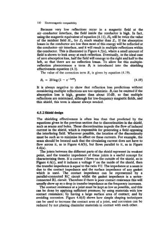
110   Electromagnetic compatibility
                          Because  very  low  reflections  occur  in  a  magnetic  field  at  the
                        air-conductor  interface, the field inside the conductor is high.  In fact,
                        using the magnetic equivalent  of equation (4.11), H2 will be twice the value
                       of  the incident field HI, for Z2 much smaller than Z1. the absorption
                                                                         If
                        losses in the conductor are low then most of this energy will be reflected at
                        the conductor-air  interface, and it will result in multiple reflections within
                        the conductor. This is illustrated in Figure 4.S(e), where a small amount of
                        field is shown to leak away at each reflection. Eventually, in the ideal case
                        of zero absorption loss, half the field will emerge to the right and half to the
                       left,  so that  there  are no  reflection losses. To allow for this multiple-
                       reflection  phenomenon  a  term  BI  is  introduced  into  the  shielding
                       effectiveness equation (4.3).
                          The value of the correction term B, is given by equation (4.19).
                         B,  = 20 log (1 - e-w6)                                  (4.19)

                       It  is  always  negative  to  show  that  reflection  loss  predictions  without
                       considering multiple reflections are too optimistic. BI can be omitted if the
                       absorption  loss  is  high, greater  than  about  lOdB,  so  that  multiple
                       reflections are minimised, although for low-frequency magnetic fields, and
                       thin shield, this term is almost always needed.


                       4.5.2  Shield design
                       The  shielding  effectiveness  is  often  less  than  that  predicted  by  the
                       equations given in the previous section due to discontinuities in the shield,
                       such as seams and holes. These discontinuities impede the flow of induced
                       current in the shield, which is responsible for generating a field opposing
                       the interfering field. Wherever possible, the location of  the discontinuity
                       must be such as to minimise its effect on these currents. For example, the
                       seam should be located such that the circulating current does not have to
                       flow across it, as in Figure 4.6(b),  but flows parallel to it, as in Figure
                       4.6(a).
                         The joints between the different parts of  the shield represent its weakest
                       point, and the transfer impedance of  these joints is a useful concept for
                       characterising them. If  a current Z flows on the outside of the shield, as in
                       Figure 4.6(c),  and it induces a voltage V on the inside of  the shield, then
                       the transfer impedance is equal to the ratio VU. The impedance at a seam is
                       due to the contact impedance and the surface impedance of  any gasket
                       which  is  used.  The  contact  impedance  can  be  represented  by  a
                       parallel-connected RC circuit whilst  the  gasket  impedance  is  a  series-
                       connected RL circuit. Therefore if there is poor contact resistance this will
                       usually show up as a drop in transfer impedance as the frequency increases.
                         The contact resistance at a joint must be kept as low as possible, and this
                       can be done by  applying sufficient pressure; by  using materials with low
                       contact resistance;  by  having  a  large  surface  area  of  contact;  and  by
                       avoiding corrosion. Figure 4.6(d)  shows how  simple shaping techniques
                       can be used to increase the contact area of  a joint, and corrosion can be
                       reduced by not placing dissimilar materials in contact with each other.