
Page 112 - Power Electronics Handbook
P. 112
EM1 shielding techniques 105
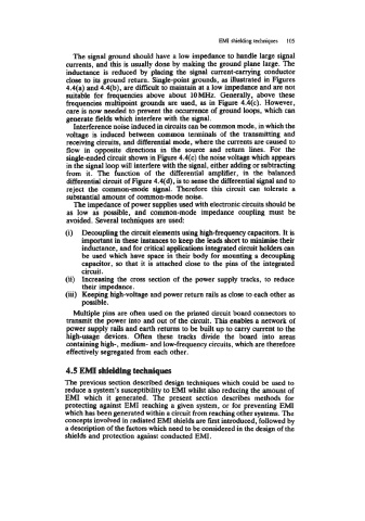
The signal ground should have a low impedance to handle large signal
currents, and this is usually done by making the ground plane large. The
inductance is reduced by placing the signal current-carrying conductor
close to its ground return. Single-point grounds, as illustrated in Figures
4.4(a) and 4.4(b), are difficult to maintain at a low impedance and are not
suitable for frequencies above about 1OMHz. Generally, above these
frequencies multipoint grounds are used, as in Figure 4.4(c). However,
care is now needed to prevent the occurrence of ground loops, which can
generate fields which interfere with the signal.
Interference noise induced in circuits can be common mode, in which the
voltage is induced between common terminals of the transmitting and
receiving circuits, and differential mode, where the currents are caused to
flow in opposite directions in the source and return lines. For the
singleended circuit shown in Figure 4.4(c) the noise voltage which appears
in the signal loop will interfere with the signal, either adding or subtracting
from it. The function of the differential amplifier, in the balanced
differential circuit of Figure 4.4(d), is to sense the differential signal and to
reject the wmmon-mode signal. Therefore this circuit can tolerate a
substantial amount of common-mode noise.
The impedance of power supplies used with electronic circuits should be
as low as possible, and common-mode impedance coupling must be
avoided. Several techniques are used:
(i) Dewupling the circuit elements using high-frequency capacitors. It is
important in these instances to keep the leads short to minimise their
inductance, and for critical rrpplications integrated cirmit holders can
be used which have space in their body for mounting a decoupiing
capacitor, so that it is attached close to the pins of the integrated
circuit.
(ii) Increasing the cross section of the power supply tracks, to reduce
their impedance.
(iii) Keeping high-voltage and power return rails as close to each other as
possible.
Multiple pins are often used on the printed circuit board connectors to
transmit the power into and out of the circuit. This enables a network of
power supply rails and earth returns to be built up to carry current to the
high-usage devices. Often these tracks divide the board into areas
containing high-, medium- and low-frequency circuits, which are therefore
effectively segregated from each other.
4.5 EMI shielding techniques
The previous section described design techniques which could be used to
reduce a system’s susceptibility to EMI whilst also reducing the amount of
EMI which it generated. The present section describes methods for
protecting against EM1 reaching a given system, or for preventing EM1
which has been generated within a circuit from reaching other systems. The
concepts involved in radiated EMI shields are first introduced, followed by
a description of the factors which need to be considered in the design of the
shields and protection against conducted EMI.