
Page 175 - Power Electronics Handbook
P. 175
Phase control 167
Gate To power
lines Delay driver ' ' semiconductors
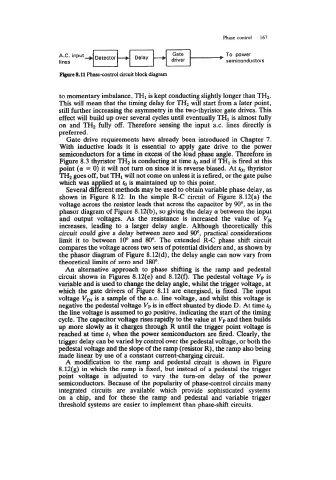
Figure 8.11 Phase-control circuit block diagram
to momentary imbalance, TH1 is kept conducting slightly longer than TH2.
This will mean that the timing delay for TH2 will start from a later point,
still further increasing the asymmetry in the two-thyristor gate drives. This
effect will build up over several cycles until eventually THI is almost fully
on and TH2 fully off. Therefore sensing the input ax. lines directly is
preferred.
Gate drive requirements have already been introduced in Chapter 7.
With inductive loads it is essential to apply gate drive to the power
semiconductors for a time in excess of the load phase angle. Therefore in
Figure 8.3 thyristor TH2 is conducting at time to and if THl is fired at this
point (a = 0) it will not turn on since it is reverse biased. At to1 thyristor
TH2 goes off, but TH1 will not come on unless it is refired, or the gate pulse
which was applied at r,, is maintained up to this point.
Several different methods may be used to obtain variable phase delay, as
shown in Figure 8.12. In the simple R-C circuit of Figure 8.12(a) the
voltage across the resistor leads that across the capacitor by !No, as in the
phasor diagram of Figure 8.12(b), so giving the delay a between the input
and output voltages. As the resistance is increased the value of VR
increases, leading to a larger delay angle. Although theoretically this
circuit could give a delay between zero and W, practical considerations
limit it to between 10" and 80'. The extended R-C phase shift circuit
compares the voltage across two sets of potential dividers and, as shown by
the phasor diagram of Figure 8.12(d), the delay angle can now vary from
theoretical limits of zero and 180".
An alternative approach to phase shifting is the ramp and pedestal
circuit shown in Figures 8.12(e) and 8.12(f). The pedestal voltage Vp is
variable and is used to change the delay angle, whilst the trigger voltage, at
which the gate drivers of Figure 8.11 are energised, is fixed. The input
voltage Vm is a sample of the a.c. line voltage, and whilst this voltage is
negative the pedestal voltage Vp is in effect shunted by diode D. At time to
the line voltage is assumed to go positive, indicating the start of the timing
cycle. The capacitor voltage rises rapidly to the value at Vp and then builds
up more slowly as it charges through R until the trigger point voltage is
reached at time tl when the power semiconductors are fired. Clearly, the
trigger delay can be varied by control over the pedestal voltage, or both the
pedestal voltage and the slope of the ramp (resistor R), the ramp also being
made linear by use of a constant current-charging circuit.
A modification to the ramp and pedestal circuit is shown in Figure
8.12(g) in which the ramp is fixed, but instead of a pedestal the trigger
point voltage is adjusted to vary the turn-on delay of the power
semiconductors. Because of the popularity of phase-control circuits many
integrated circuits are available which provide sophisticated systems
on a chip, and for these the ramp and pedestal and variable trigger
threshold systems are easier to implement than phase-shift circuits.