
Page 191 - Principles and Applications of NanoMEMS Physics
P. 191
4. NANOMEMS APPLICATIONS: CIRCUITS AND SYSTEMS 179
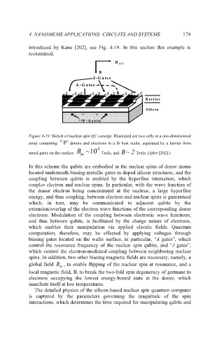
introduced by Kane [202], see Fig. 4-19. In this section this example is
reexamined.
B B AC
AC
B B B
J-G a
J-G a te t
J-G a te s s e s
A-G a te s s e s
A-G a
A-G a te t
B a rrie e
B a rri
B a rrie r r r
S ilic o o
S ilic
S ilic o n n n
e - e - e - e - e - e -
31 P P P + Q ubi
+ Q ubit t
+ Q ubits s s
31
31
Figure 4-19. Sketch of nuclear spin QC concept. Illustrated are two cells in a one-dimensional
31 +
array containing P donors and electrons in a Si host wafer, separated by a barrier from
3 −
metal gates on the surface. B ac ~ 10 Tesla, and ~B 2 Tesla. (After [202].)
In this scheme the qubits are embodied in the nuclear spins of donor atoms
located underneath biasing metallic gates in doped silicon structures, and the
coupling between qubits is enabled by the hyperfine interaction, which
couples electron and nuclear spins. In particular, with the wave function of
the donor electron being concentrated at the nucleus, a large hyperfine
energy, and thus coupling, between electron and nuclear spins is guaranteed
which, in turn, may be communicated to adjacent qubits by the
extension/overlap of the electron wave functions of the corresponding donor
electrons. Modulation of the coupling between electronic wave functions,
and thus between qubits, is facilitated by the charge nature of electrons,
which enables their manipulation via applied electric fields. Quantum
computation, therefore, may be effected by applying voltages through
biasing gates located on the wafer surface, in particular, “A gates”, which
control the resonance frequency of the nuclear spin qubits, and “J gates”,
which control the electron-mediated coupling between neighboring nuclear
spins. In addition, two other biasing magnetic fields are necessary, namely, a
global field B , to enable flipping of the nuclear spin at resonance, and a
ac
local magnetic field, B, to break the two-fold spin degeneracy of germane to
electrons occupying the lowest energy-bound state at the donor, which
manifests itself at low temperatures.
The detailed physics of the silicon-based nuclear spin quantum computer
is captured by the parameters governing the magnitude of the spin
interactions, which determines the time required for manipulating qubits and