
Page 212 - Principles and Applications of NanoMEMS Physics
P. 212
5. NANOMEMS APPLICATIONS: PHOTONICS 201
5.3.2.3 SP Resonances in Single Metallic Nanoparticles
Further efforts were made to study the confinement of SPs to metallic
nanoparticles. Among these, Klar et al. [217] reported the measurement of
SP resonances in single metallic nanoparticles, and of the homogeneous line
shape of their resonance, via photon scanning tunneling microscopy (PSTM)
(PSTM detects a signal at the exit of an optical fiber tip that is proportional
to the near field.) These SP resonances are known to be determined by the
dielectric properties of the medium in which the particles are embedded, and
by the size and shape of the particles, and are accompanied by a large
resonant enhancement of the local field both inside and near the particle, see
Fig. 5-6 [218].
Ionic C luster r
Ionic C luste
Surface C harge
Surface C harges s
+ + + + + + + + -- --
+ + + + - - - - - - - -
Ligh
Light t
- - - - + + + +
E lectric F ield - - -- - - + + + + + + + +
E lectric F ield
--
E lectronic C luste
E lectronic C luster r
Tim e t t
Tim e T im e t+T/2
T im e t+T/2
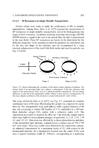
Figure 5-6. Sketch illustrating the excitation of the dipole surface plasmon oscillation. The
electric field of an incoming light wave induces a polarization of the free electrons with
respect to the much heavier ionic core of a spherical metallic nanoparticle. The net charge
difference is only felt at the nanoparticle surface which, in turn, acts as a restoring force. In
this way a dipolar oscillation of the electrons is created with period T.(After [218].)
The setup utilized by Klar et al. [217], see Fig. 5-7, consisted of a tunable
continuous wave (CW) laser illuminating the sample via a tapered Al-coated
fiber tip. The nanoparticles were gold spheres with a typical diameter of 40
nm, and occupying a volume fill fraction of 3 %, embedded in a 200 nm-
thick dielectric sol-gel TiO 2 matrix with a refractive index 2.19. The
experiment proceeded to position the fiber tip 7 nm from the sample and to
shine laser light of various photon energies, in particular, 2,11 eV, 2 eV, 1.94
eV, and 1.91 eV. Detection was effected by a silicon photodetector and plots
of the transmitted light intensity, scanned across a surface area of 750 x 750
2
nm were made. Three key results were obtained in the experiment, namely,
an enhanced transmission by a maximum factor of 12, with respect to the
background intensity, for a nanoparticle located near the center of the scan
area, a typical resonance width of ~160meV, corresponding to a dephasing