
Page 216 - Principles and Applications of NanoMEMS Physics
P. 216
5. NANOMEMS APPLICATIONS: PHOTONICS 205
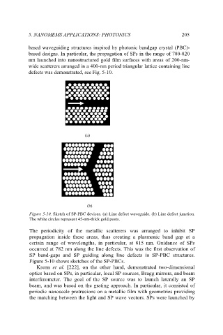
based waveguiding structures inspired by photonic bandgap crystal (PBC)-
based designs. In particular, the propagation of SPs in the range of 780-820
nm launched into nanostructured gold film surfaces with areas of 200-nm-
wide scatterers arranged in a 400-nm period triangular lattice containing line
defects was demonstrated, see Fig. 5-10.
(a)
(b)
Figure 5-10. Sketch of SP-PBC devices. (a) Line defect waveguide. (b) Line defect junction.
The white circles represent 45-nm-thick gold posts.
The periodicity of the metallic scatterers was arranged to inhibit SP
propagation inside these areas, thus creating a plasmonic band gap at a
certain range of wavelengths, in particular, at 815 nm. Guidance of SPs
occurred at 782 nm along the line defects. This was the first observation of
SP band-gaps and SP guiding along line defects in SP-PBC structures.
Figure 5-10 shows sketches of the SP-PBCs.
Krenn et al. [222], on the other hand, demonstrated two-dimensional
optics based on SPs, in particular, local SP sources, Bragg mirrors, and beam
interferometer. The goal of the SP source was to launch laterally an SP
beam, and was based on the grating approach. In particular, it consisted of
periodic nanoscale protrusions on a metallic film with geometries providing
the matching between the light and SP wave vectors. SPs were launched by