Page 218 - Principles and Applications of NanoMEMS Physics
P. 218
5. NANOMEMS APPLICATIONS: PHOTONICS                           207

             by combining two Bragg mirrors symmetrically with respect to a nanowire
             used for launching SPs, see Fig. 5-11.

             5.3.4   Semiconducting Nanowire-Based Nanophotonics

                In addition to the SP-based nanophotonics approach, an approach based
             on using active nanowire waveguides has been advanced by Lieber’s group
             [216]. This  approach  is motivated by  an attempt  to circumvent the loss
             limitations exhibited by passive waveguides, such as  SP-based devices,
             which may hinder their applicability for manipulating light over the extent of
             integrated photonic systems.
                Early  examples of semiconducting nanowires include nanoscale lasers
             [223], in  which a sub-wavelength  diameter  nanocavity is  created  by
             exploiting the  high refractive  index  contrast  between a nanowire and its
             surroundings.  The  active  waveguide concept  pursued by Lieber’s group
             [216] involves utilizing cavities such as these as waveguides. The feasibility
             of the concept was investigated by quantitatively characterizing the  losses
             through straight and sharply bent CdS nanowires, of sub-wavelength (200
             nm) diameter, by scanning optical microscopy. In particular, the experiments
             recorded spatial maps of the intensity of light emitted from one end of the
             nanowire, as a function of the position of a diffraction-limited laser spot with
             energy  greater than the CdS band  gap.  In this context,  the laser energy
             absorbed  by  the  CdS  nanowire was re-emitted via photoluminescence and
             subsequently guided by it. The  experiment indicated that active CdS
             nanowires are capable of efficient guiding over straight and sharp and acute
             angle bends,  with typical  losses of about 1-2dB in  an abrupt  bend.  In
             addition, by studying the characteristics of junctions between two nanowires
             it was found that light may be coupled efficiently through sub-wavelength
             bends defined by them. Finally, by applying a variable electric field across a
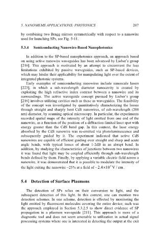
             nanowire, it was demonstrated that it is possible to modulate the intensity of
             the light exiting the nanowire ~25% at a field of ~ 4.2 × 10  5  V  /  cm .


             5.4  Detection of Surface Plasmons

                The  detection of  SPs relies on their conversion to light, and  the
             subsequent detection of  this  light.  In this context,  one can  mention two
             detection  schemes. In one scheme, detection is effected by monitoring the
             light emitted by fluorescent molecules covering the entire device; such was
             the  approach  employed  in Section 5.3.2.5 to show direct  evidence of SP
             propagation  in  a  plasmon waveguide [211]. This approach is more  of  a
             diagnostic tool and does not seem amenable to utilization in actual  signal
             processing systems where one is interested in detecting the output at the exit

