
Page 11 - Radar Technology Encyclopedia
P. 11
ABSORBER, radar absorber, Dahlenbach 1
A conductivity of the deposition on the film. An example of a
pattern deposited on a CA sheet in shown in Fig. A1.
CA absorbers can be tuned, as with an RLC circuit,
ABSORBER, radar. The term absorber refers to a radar-
enabling the designer to improve the bandwidth of the multi-
absorbing structure or material (RAS or RAM), the purpose
sheet configuration. In general, CA absorber is a lossy ver-
of which is to soak up incident energy and reduce the energy
sion of a class of printed patterns known as frequency-
reflected back to the radar. Its main objective is to achieve
selective surfaces (FSS). SAL
reduction in the radar cross section (RCS) of radar targets.
Other applications are to suppress wall reflections in anechoic Ref.: Knott (1993) p. 326; Bhattacharyya (1991), pp. 215–217.
chambers and reflections from nearby structures at fixed
radar sites.
Absorbers can be classified from the point of view of
scattering phenomena as specular and nonspecular types, and
from the point of view of their bandwidth as narrowband
RAS and wideband RAS. The major representatives of nar-
rowband RAS are the Salisbury screen and the Dahlenbach
absorber. Wideband RAS are represented by m = e type
r
r
absorbers, circuit analog absorbers, frequency-selective sur-
faces, geometric transition absorbers, Jaumann absorbers, and
graded absorbers. Some of these types can be combined to
form hybrid absorbers with improved performance. All these
types are specular absorbers designed to reduce specular
reflections from metallic surfaces. Nonspecular absorbers are
intended primarily for suppression of surface traveling-wave
echoes. SAL
Figure A1 Circuit analog absorbers (after Knott, 1993,
Absorbers for anechoic chambers are applied to the internal Fig. 8.18, p. 326).
surfaces of an anechoic chamber to absorb the incident radio
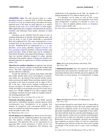
A Dahlenbach absorber (Fig. A2) consists of a thick homo-
waves. The basic requirements are wideband performance
geneous lossy layer backed by a metallic plate. It is a simple
and low reflection coefficient.
narrowband absorber that is flexible and can be applied to dif-
Usually the absorber is a plastic foam frame with filler
ferent kinds of curved surfaces. It is characteristic of single-
that readily absorbs radio waves (microspheres of polysty-
rene, teflon, etc.), the density of the material and the concen- e , m
tration growing with depth. Radar-absorbing material is most
convenient in the form of pyramids with an angle of 30° to
60°at the apex, which assures multiple re-reflections that q
increase absorption. To reduce the reflection coefficient to -
q
20 dB, the height of the pyramids must be 0.5l to 0.6l, but to
reduce it to -50 dB, a height of 7l to 10l is required. In this L
case thinner structures are used, made, for example, from fer-
rite absorbing materials. IAM
Z = 0 Z = L
Ref.: Finkel'shteyn (1983), p. 145; Knott, 1993, pp. 528–532.
Chirosorb absorbing material is a novel RAM typically Figure A2 Dahlenbach absorber (after Bhattacharyya, 1991,
fabricated by embedding randomly oriented identical chiral Fig. 4.65, p. 211).
microstructures (e.g., microhelices), in an isotropic host layer absorbers backed by metal plates that it is impossible to
medium. In comparison with conventional RAMs, it pos- achieve zero reflection because the layer material must be
sesses an excellent low-reflectivity property and may be prac- such that low reflection occurs on its front face, and using
tically invisible to radar. SAL physically realizable materials it is impossible to force reflec-
Ref.: Bhattacharyya (1991), p. 233. tion from both the front face and the metal backing to zero.
Circuit analog (CA) absorbers are sheets of low-loss mate- The main objective in this case is to choose electrical proper-
rial on which specific conducting patterns have been depos- ties of the layer to make two reflections to cancel each other.
ited. The patterns constitute resistance, inductance, and Reflectivity curves for dominantly electrical and magnetic
capacitance. The deposited film can be represented by an layer materials are shown in Figs. A3 and A4, respectively.
equivalent RLC circuit, parameters of which can be con- The optimum layer thickness in the first case is near a quarter
trolled by the geometric configuration, film thickness, and wavelength, in the second case it is near a half wavelength.
SAL
Ref.: Knott (1993), pp. 314–320; Bhattacharyya (1991), pp. 208–212.