
Page 172 - Rashid, Power Electronics Handbook
P. 172
10 Diode Recti®ers 161
the assumption that transformer T effectively has no leakage MOS transistor Vð3Þ is found to be acceptable. However, there
1
inductance (with coupling coef®cient K ¼ 0:99999999). are still large ringing voltages across the output recti®ers
However, it is found that when a practical transformer (Vð6; 9Þ and Vð9Þ).
(having a slightly lower K) is used, severe ringings occur. To damp the ringing voltages across the output recti®ers,
Fig. 10.32 shows some simulation results to demonstrate this additional snubber circuits across the recti®ers may therefore
phenomenon and the following assumptions are made: also be required in a practical circuit, as will be described in
what follows.
D and D are MBR2540 Schottky diodes and D M is an
R
F
MUR460 ultra fast diode;
M is an IRF640 MOS transistor; 10.6.1.6 Practical Circuit
1
transformer T has a practical coupling coef®cient of
1
0.996; Fig. 10.35 shows a practical forward converter also with
snubber circuits added to recti®ers (R C for D and R C
the effective winding resistance of L is 0:1 O, the 2 2 R 3 3
P
effective winding resistance of L is 0:4 O, and the for D ) to reduce voltage ringing. Figs. 10.36 and 10.37 show
F
M
effective winding resistance of L is 0:01 O; the resultant voltage and current waveforms. Fig. 10.36 is for
S
the effective series resistance of the output ®ltering continuous-mode operation (R ¼ 0:35 O), where IðL Þ
1
L
(current in L ) is continuous. Figure 10.37 is for discontin-
capacitor is 0:05 O; and 1
uous-mode operation (R ¼ 10 O), where IðL Þ becomes
the switching operation of the converter has reached a L 1
discontinuous due to an increased value of R . These wave-
steady state. L
forms are considered to be acceptable.
The resultant waveforms shown in Fig. 10.32 indicate that The design considerations of diode recti®er circuits in high-
there are large voltage and current ringings in the circuit. frequency converters will be discussed later in Section 10.6.3.
These ringings are caused by the resonant circuits formed by
the leakage inductance of the transformer and the parasitic
capacitances of the diodes and the transistor. 10.6.2 Flyback Rectifier Diode and Clamping
Therefore, a practical converter may need snubber circuits Diode in a Flyback Converter
to damp these ringings, as will be described in what follows.
10.6.2.1 Ideal Circuit
10.6.1.5 Circuit with Snubber Across Transformer Fig. 10.38 shows the basic circuit of a ¯yback converter. Due to
its simple circuit, this type of converter is widely used in low-
To suppress the ringing voltage caused by the resonant circuit
cost low-power applications. Discontinuous-mode operation
formed by transformer leakage inductance and the parasitic
capacitance of the MOS switch, a snubber circuit, shown as R 1 (meaning that the magnetizing current in the transformer falls
and C in Fig. 10.33, is now connected across the primary to zero before the end of each switching cycle) is often used
1
winding of transformer T . The new waveforms are shown in because it offers the advantages of easy control and low diode
1
Fig. 10.34. Here the drain-to-source voltage waveform of the reverse-recovery loss. Fig. 10.39 shows the idealized steady-
state waveforms for discontinuous-mode operation. These
waveforms are obtained from PSpice simulations, based on
the following assumptions:
D is an idealized recti®er diode with in®nitely fast
R
switching speed;
M 1 is an idealized MOS switch with in®nitely fast
switching speed, with on-state resistance of 0:067 O;
and off-state resistance of 1 MO;
transformer T has a coupling coef®cient of 0.99999999;
1
and
the switching operation of the converter has reached a
steady state.
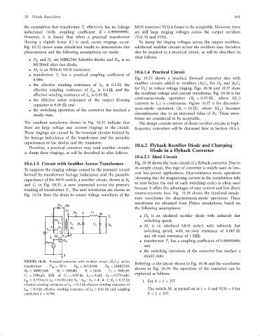
FIGURE 10.33 Forward converter with snubber circuit (R 1 C 1 ) across
Referring to the circuit shown in Fig. 10.38 and the waveforms
transformer: V IN ¼ 50 V; D M ¼ MUR460; D R ¼ MBR2540;
shown in Fig. 10.39, the operation of the converter can be
D F ¼ MBR2540; M 1 ¼ IRF640; R 1 ¼ 24 O; C 1 ¼ 3000 pF;
explained as follows:
C L ¼ 3500 mF; ESR of C L ¼ 0:05 O; L 1 ¼ 8 mH; L P ¼ 0:576 mH;
L M ¼ 0:576 mH; L S ¼ 0:036 mH; N P : N M : N S ¼ 4 : 4 : 1; R L ¼ 0:35 O; 1. For 0 < t < DT
effective winding resistance of L P ¼ 0:1 O; effective winding resistance of
L M ¼ 0:4 O; effective winding resistance of L S ¼ 0:01 O; and coupling The switch M is turned on at t ¼ 0 and Vð3Þ¼ 0 for
1
coef®cient k ¼ 0:996. 0 < t < DT.