
Page 177 - Rashid, Power Electronics Handbook
P. 177
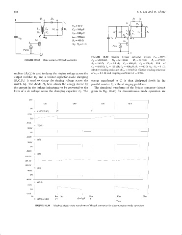
166                                                                                 Y.-S. Lee and M. Chow


                                                                    FIGURE  10.40  Practical  ¯yback  converter  circuit:  V IN ¼ 60 V;
                       FIGURE 10.38  Basic circuit of ¯yback converter.  D S ¼ MUR460;  D R ¼ MUR460;  M 1 ¼ IRF640;  R 1 ¼ 4:7 KO;
                                                                    R 2 ¼ 100 O;  C 1 ¼ 0:1 mF;  C 2 ¼ 680 pF;  C L ¼ 100 mF;  ESR  of
                                                                    C L ¼ 0:05 O; L p ¼ 100 mH; L S ¼ 400 mH; R L ¼ 400 O; N P : N S ¼ 1 : 2;
                                                                    effective winding resistance of L P ¼ 0:025 O; effective winding resistance
               snubber (R C ) is used to damp the ringing voltage across the  of L S ¼ 0:1 O; and coupling coef®cient K ¼ 0:992.
                        2  2
               output recti®er D and a resistor-capacitor-diode clamping
                              R
               (R C D ) is used to clamp the ringing voltage across the  energy transferred to C is then dissipated slowly in the
                 1 1  S                                                                  1
               switch M . The diode D here allows the energy stored by  parallel resistor R without ringing problems.
                       1            S                                             1
               the current in the leakage inductance to be converted to the  The simulated waveforms of the ¯yback converter (circuit
               form of a dc voltage across the clamping capacitor C . The  given in Fig. 10.40) for discontinuous-mode operation are
                                                             1


                              FIGURE 10.39  Idealized steady-state waveforms of ¯yback converter for discontinuous-mode operation.