Page 181 - Rashid, Power Electronics Handbook
P. 181

170                                                                           J. Rodrõ Âguez and A. Weinstein

                                            Area A                                           T1
                                          v     1
                          v   i            d  v  Area A
                         +  L  -  d          R     2                              i s     v 1  v T1  i T1
                                                  R
                      i  +  L      0             v ,v  d       wt           v  +           N 2       i d
                  +   G      +              p        2p                      s                  N
                 v              R               v  v                                      v           R   v
                  s    v d    -              v d  d  s                                     2  T2  i       d
                  -                                                                  N 1         T2
                         -             i G                                                    v
                                   0                           wt                             T2
                                  a)                                          i               i
                                                                              s               s
                                          Area A
                                              1
                          v   i            v  Area A
                         +  L  -  d         d     2 v d
                      i  +  L           i d      E d  i                              N 2              N 2
                  +   G      +      0                          wt               i = i ·         i = i ·
                                                                                                 s
                                                                                                    T2
                                                                                s
                                                                                   T1
                 v              E           v        2p                              N 1    v         N 1
                  s    v d   -   d          d       v                                        d
                  -                                  s              V max
                         -              i G
                                    0                          wt      0                                            wt
                                  b)
                                                                                           v          -v
                                                                                            s          s
                                                                     i
               FIGURE 11.2  Single thyristor recti®er with: (a) resistive-inductive load;  g1  a
               and (b) active load.                                    0                                            wt
                                                                     i g2
                 When an inductive-active load is connected to the recti®er,  0                                     wt
               as depicted in Fig. 11.2b, the thyristor will be turned ON if the  i T1
               ®ring pulse is applied to the gate when v > E . Again, the  0                                        wt
                                                   s   d
               thyristor will remain in the ON state until A ¼ A . When the
                                                   1    2
               thyristor is turned OFF, the load voltage will be v ¼ E .  i T2
                                                        d    d
                                                                       0                                            wt
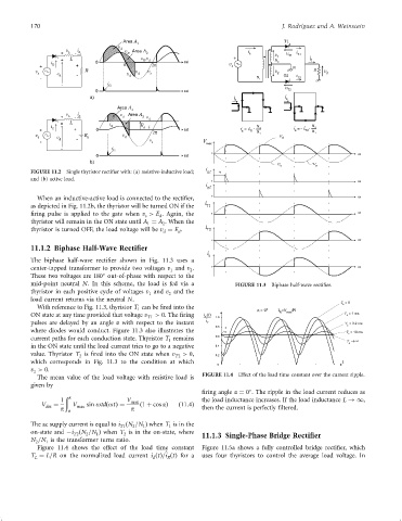
               11.1.2 Biphase Half-Wave Rectifier
                                                                      i s
               The biphase half-wave recti®er shown in Fig. 11.3 uses a
               center-tapped transformer to provide two voltages v and v .  0                                       wt
                                                                2
                                                          1

               These two voltages are 180 out-of-phase with respect to the
               mid-point neutral N. In this scheme, the load is fed via a     FIGURE 11.3  Biphase half-wave recti®er.
               thyristor in each positive cycle of voltages v and v and the
                                                    1     2
               load current returns via the neutral N.
                                                                                                               T L =0
                 With reference to Fig. 11.3, thyristor T can be ®red into the
                                                1                                    a=0º   î =V  /R
               ON state at any time provided that voltage v  > 0. The ®ring  i d t)(        R  max              T L =1ms
                                                   T1                   1.0
               pulses are delayed by an angle a with respect to the instant  R i ˆ                              T L = 3.2 ms
                                                                        0.8  2
               where diodes would conduct. Figure 11.3 also illustrates the  p                                  T L =10ms
               current paths for each conduction state. Thyristor T remains  0.6
                                                          1
                                                                                                                 T L
               in the ON state until the load current tries to go to a negative  0.4
               value. Thyristor T is ®red into the ON state when v T2  > 0,  0.2
                              2
               which corresponds in Fig. 11.3 to the condition at which                                        t
                                                                         0
               v > 0.
                2
                 The mean value of the load voltage with resistive load is  FIGURE 11.4  Effect of the load time constant over the current ripple.
               given by

                                                                    ®ring angle a ¼ 0 . The ripple in the load current reduces as
                          ð p
                         1                   V max                  the load inductance increases. If the load inductance L !1,
                   V dia  ¼  p  a  V max  sin otdðotÞ¼  p  ð1 þ cos aÞ  ð11:4Þ  then the current is perfectly ®ltered.
               The ac supply current is equal to i ðN =N Þ when T is in the
                                                  1
                                               2
                                           T1
                                                          1
               on-state and ÿi ðN =N Þ when T is in the on-state, where  11.1.3 Single-Phase Bridge Rectifier
                                    1
                             T2
                                2
                                            2
               N =N is the transformer turns ratio.
                 2
                    1
                 Figure 11.4 shows the effect of the load time constant  Figure 11.5a shows a fully controlled bridge recti®er, which
                                                         ^
               T ¼ L=R on the normalized load current i ðtÞ=i ðtÞ for a  uses four thyristors to control the average load voltage. In
                 L
                                                     d
                                                         R
   176   177   178   179   180   181   182   183   184   185   186