Page 182 - Rashid, Power Electronics Handbook
P. 182

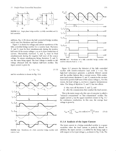
11  Single-Phase Controlled Recti®ers                                                               171

                                   i                        i
                        i T1       d                         d          V
                                P                         P               max
                       i g1                     i g1
                            T                         T
                       T     3                   T    2
                        1                         1                        0                                         wt
                               i T3
                    +  i                     +  i
                  v    s         v    Load  v   s         v     Load
                   s             d           s             d
                                                                                              v         -v
                                                                          i                    s          s
                       T    T                    D    D                    d
                        4    2                    1   2
                                N                        N                            I
                        i T4                                                           d
                                                                           0                                         wt
                             a)                        b)              i ,i   a
                                                                       g1  g2
                 FIGURE 11.5  Single-phase bridge recti®er: (a) fully controlled; and (b)  0                         wt
                                                                       i ,i
                 half controlled.                                      g3  g4
                                                                           0                                         wt
                                                                       i ,i
                                                                       T1 T2
                 addition, Fig. 11.5b shows the half-controlled bridge recti®er,
                 which uses two thyristors and two diodes.                                                           wt
                                                                           0
                   Figure 11.6 shows the voltage and current waveforms of the  i ,i
                 fully controlled bridge recti®er for a resistive load. Thyristors  T3 T4
                 T and T must be ®red simultaneously during the positive   0                                         wt
                         2
                   1
                 half wave of the source voltage v so as to allow conduction of
                                            s
                 current. Alternatively, thyristors T and T must be ®red  i s
                                                      4
                                               3
                 simultaneously during the negative half wave of the source  0                                       wt
                 voltage. To ensure simultaneous ®ring, thyristors T and T
                                                            1      2  FIGURE 11.7  Waveforms of a fully controlled bridge recti®er with
                 use the same ®ring signal. The load voltage is similar to the
                                                                      resistive-inductive load (L !1).
                 voltage obtained with the biphase half-wave recti®er. The
                 input current is given by
                                                                        Figure 11.7 presents the behavior of the fully controlled
                                     i ¼ i T1  ÿ i T4          ð11:5Þ  recti®er with resistive-inductive load (with L !1). The
                                      S
                                                                      high-load inductance generates a perfectly ®ltered current
                 and its waveform is shown in Fig. 11.6.
                                                                      and the recti®er behaves like a current source. With contin-
                                                                      uous load current, thyristors T and T remain in the on-state
                                                                                                     2
                                                                                               1
                                          v                           beyond the positive half-wave of the source voltage v . For this
                                           d                                                                    s
                    V                                                 reason, the load voltage v can have a negative instantaneous
                     max                                                                   d
                                                                      value. The ®ring of thyristors T and T has two effects:
                                                                                                3
                                                                                                      4
                       0                                        wt
                                                                          i) they turn off thyristors T and T ; and
                                                                                                 1
                                                                                                        2
                                          v         -v
                                           s          s                   ii) after the commutation they conduct the load current.
                   i ,i
                   g1  g2 a
                                                                        This is the main reason why this type of converter is called a
                       0                                        wt    ‘‘naturally commutated'' or ‘‘line commutated'' recti®er. The
                  i ,i
                   g3  g4                                             supply current i has the square waveform shown in Fig. 11.7
                                                                                   S
                       0                                        wt    for continuous conduction. In this case, the average load
                  i  ,i                                               voltage is given by
                  T1  T2
                                                                wt
                       0
                                                                                  ð pþa
                  i  ,i                                                         1                     2V max
                  T3  T4                                                  V dia  ¼    V max  sin otdðotÞ¼  cos a   ð11:6Þ
                                                                                p  a                    p
                       0                                        wt
                      i
                      s                                               11.1.4 Analysis of the Input Current
                       0                                        wt
                                                                      The input current in a bridge-controlled recti®er is a square
                                                                      waveform when the load current is perfectly ®ltered. In
                 FIGURE 11.6  Waveforms of a fully controlled bridge recti®er with  addition, the input current i is shifted by the ®ring angle a
                                                                                              s
                 resistive load.                                      with respect to the input voltage v , as shown in Fig. 11.8a. The
                                                                                                 s
   177   178   179   180   181   182   183   184   185   186   187