Page 184 - Rashid, Power Electronics Handbook
P. 184

11  Single-Phase Controlled Recti®ers                                                               173

                 distortion of the current produces an increase in the value of I s  During commutation the following expression holds:
                 in Eq. (11.16), which deteriorates the power factor.
                                                                           di s
                                                                          L   ¼ v ¼ V max  sin ot  a   ot   a þ m  ð11:18Þ
                                                                                 s
                                                                            dt
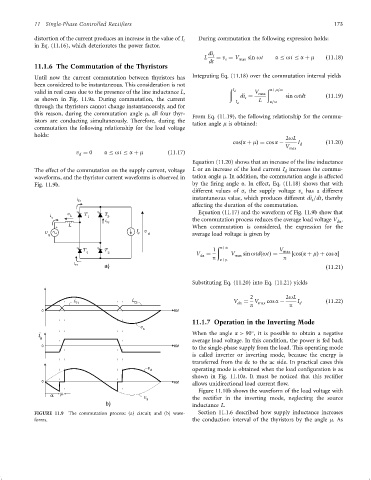
                 11.1.6 The Commutation of the Thyristors
                 Until now the current commutation between thyristors has  Integrating Eq. (11.18) over the commutation interval yields
                 been considered to be instantaneous. This consideration is not
                                                                                  ð I d        ð aþm=o
                 valid in real cases due to the presence of the line inductance L,         V max
                                                                                      di ¼           sin otdt      ð11:19Þ
                 as shown in Fig. 11.9a. During commutation, the current                s   L
                                                                                   ÿI d         a=o
                 through the thyristors cannot change instantaneously, and for
                 this reason, during the commutation angle m, all four thyr-
                                                                      From Eq. (11.19), the following relationship for the commu-
                 istors are conducting simultaneously. Therefore, during the
                                                                      tation angle m is obtained:
                 commutation the following relationship for the load voltage
                 holds:
                                                                                                     2oL
                                                                                    cosða þ mÞ¼ cos a ÿ  I d       ð11:20Þ
                                                                                                     V max
                               v ¼ 0     a   ot   a þ m       ð11:17Þ
                                d
                                                                      Equation (11.20) shows that an increase of the line inductance
                 The effect of the commutation on the supply current, voltage  L or an increase of the load current I increases the commu-
                                                                                                     d
                 waveforms, and the thyristor current waveforms is observed in  tation angle m. In addition, the commutation angle is affected
                 Fig. 11.9b.                                          by the ®ring angle a. In effect, Eq. (11.18) shows that with
                                                                      different values of a, the supply voltage v has a different
                                                                                                          s
                                i T1                                  instantaneous value, which produces different di =dt, thereby
                                                                                                              s
                                                                      affecting the duration of the commutation.
                       i    v L   T      T                              Equation (11.17) and the waveform of Fig. 11.9b show that
                       s           1     i  3                         the commutation process reduces the average load voltage V .
                                                                                                                      da
                             L           T3                           When commutation is considered, the expression for the
                         +
                     v                             I d  v
                      s                                d              average load voltage is given by
                                  T      T                                   1  ð pþa              V
                                   4      2                            V   ¼       V   sin otdðotÞ¼  max  ‰cosða þ mÞþ cos aŠ
                                                                         da
                                                                             p  aþm  max            p
                               i T4      a)                                                                        ð11:21Þ
                                                                      Substituting Eq. (11.20) into Eq. (11.21) yields

                                                                                         2
                               i                  i                                 V  ¼ V     cos a ÿ  2oL  I     ð11:22Þ
                               T1                 T3                                 da  p  max       p   d
                                                                wt
                    0
                                                                      11.1.7 Operation in the Inverting Mode
                                                     v s
                   i                                                  When the angle a > 90 , it is possible to obtain a negative

                   s                                                  average load voltage. In this condition, the power is fed back
                                                                wt
                    0
                                                                      to the single-phase supply from the load. This operating mode
                                                                      is called inverter or inverting mode, because the energy is
                                                                      transferred from the dc to the ac side. In practical cases this
                                                       v
                                                        d             operating mode is obtained when the load con®guration is as
                                                                      shown in Fig. 11.10a. It must be noticed that this recti®er
                                                                wt
                    0
                                                                      allows unidirectional load current ¯ow.
                                                                        Figure 11.10b shows the waveform of the load voltage with
                       a  m                           v s             the recti®er in the inverting mode, neglecting the source
                                         b)                           inductance L.
                 FIGURE 11.9  The commutation process: (a) circuit; and (b) wave-  Section 11.1.6 described how supply inductance increases
                 forms.                                               the conduction interval of the thyristors by the angle m.As
   179   180   181   182   183   184   185   186   187   188   189