Page 188 - Rashid, Power Electronics Handbook
P. 188

11  Single-Phase Controlled Recti®ers                                                               177

                                               i                      the multiplication between the output of the voltage controller
                                                L
                                                                      and the absolute value jv ðtÞj. A hysteresis controller provides
                                                                                          s
                                                     i
                                                      L ref           a fast control for the inductor current i , resulting in a
                                                                                                          L
                                                                      practically sinusoidal input current i .
                                                                                                    s
                                                                                                   o
                          0                                t            Typically, the output voltage V should be at least 10%
                                        a)                            higher than the peak value of the source voltage v ðtÞ in order
                                                                                                              s
                                                                      to assure good dynamic control of the current. The control
                           x                                          works with the following strategy: a step increase in the
                                                                      reference voltage V  will produce an increase in the voltage
                         1                                                            oref
                                                                      error V  ÿ V and an increase of the output of the PI
                                                                            oref   o
                                                                      controller, which originates an increase in the amplitude of
                         0                                 t          the reference current i Lref . The current controller will follow
                                       b)                             this new reference and increase the amplitude of the sinusoidal
                                                                      input current i , which will increase the active power delivered
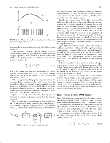
                 FIGURE 11.17  Behavior of the inductor current i L : (a) waveforms; and  s
                 (b) transistor T gate drive signal x.                by the single-phase supply and ®nally produce an increase in
                                                                      the output voltage V .
                                                                                       o
                                                                        Figure 11.19a shows the waveform of the input current i s
                 consequently, an increase in the absolute value of the source
                                                                      and the source voltage v . The ripple of the input current can
                                                                                          s
                 current i .                                          be diminished by reducing the hysteresis width d. The price to
                         s
                   When transistor T is turned OFF, the inductor current i L  be paid for this improvement is an increase in switching
                 cannot be interrupted abruptly and ¯ows through diode D,  frequency, which is proportional to the commutation losses
                 charging capacitor C. This is observed in the equivalent circuit
                                                                      of transistor T. For a given hysteresis width d, a reduction of
                 of Fig. 11.16c. In this condition the behavior of the inductor
                                                                      inductance L also produces an increase in the switching
                 current is described by
                                                                      frequency.
                                                                        A drastic reduction in the harmonic content of input
                                  di L  ¼  v L  ¼  jv jÿ V o  ð11:27Þ  current i can be observed in the frequency spectrum of Fig.
                                             s
                                                                             s
                                   dt   L      L                      11.19b. This current complies with the restrictions established
                                                                      by IEC standard 1000-3-2. The total harmonic distortion of
                 If V > jv j, which is an important condition for the correct  the current in Fig. 11.19a is THD ¼ 4.96% and the power
                     o
                          s
                 behavior of the recti®er, then jv jÿ V < 0, and this means  factor of the recti®er is PF ¼ 0.99.
                                                 o
                                            s
                 that in the OFF state the inductor current decreases its  Figure 11.20 shows the dc voltage control loop dynamic
                 instantaneous value.                                 behavior for step changes in the load. An increase in the load,
                   With an appropriate ®ring pulse sequence applied to  at t ¼ 0:3 [s], produces an initial reduction of the output
                 transistor T, the waveform of the input current i can be  voltage V , which is compensated by an increase in the input
                                                            s                 o
                 controlled to follow a sinusoidal reference, as can be observed  current i .At t ¼ 0:6 [s] a step decrease in the load is applied.
                                                                             s
                 in the positive halfwave of i in Fig. 11.17. This ®gure shows  The dc voltage controller again adjusts the supply current in
                                        s
                 the reference inductor current i  , the inductor current i ,  order to balance the active power.
                                            Lref                  L
                 and the gate drive signal x for transistor T. Transistor T is ON
                 when x ¼ ‘‘1'' and it is OFF when x ¼ ‘‘0''.
                   Figure 11.17 clearly shows that the ON(OFF) state of  11.2.4 Voltage Doubler PWM Rectifier
                 transistor T produces an increase (decrease) in the inductor
                                                                      Figure 11.21a shows the power circuit of the voltage doubler
                 current i .
                         L
                   Figure 11.18 presents a block diagram of the control system  pulsewidth modulated (PWM) recti®er, which uses two tran-
                                                                                                                    1
                                                                                                 1
                                                                                                       2
                 for the boost recti®er, which includes a proportional-integral  sistors and two ®lter capacitors C and C . Transistors T and
                                                                      T are switched in complement to control the waveform of
                                                                       2
                 (PI) controller to regulate the output voltage V . The reference  input current i and output dc voltage V . Capacitor voltages
                                                       o
                 value i Lref  for the inner current control loop is obtained from  s                  o
                                                                      V   and V  must be higher than the peak value of the input
                                                                       C1      C2
                                                                      voltage v to ensure control of the input current.
                                                                             s
                                  PI
                                                i                       The equivalent circuit of this recti®er with transistor T in
                 V                              Lref                                                                 1
                   0ref  +                        +               X
                                                            d         the ON state is shown in Fig. 11.21b. The inductor voltage
                        -                         -                   dynamic equation is
                          V                 v (t)
                           0                 s
                                            V      i
                                             max    L                                    di s
                                                                                    v ¼    ¼ v ðtÞÿ V C1  < 0      ð11:28Þ
                                                                                              s
                                                                                     L
                        FIGURE 11.18  Control system of the boost recti®er.              dt
   183   184   185   186   187   188   189   190   191   192   193