
Page 190 - Rashid, Power Electronics Handbook
P. 190
11 Single-Phase Controlled Recti®ers 179
PI i
V + sref + X In this topology, the output voltage V must be higher than
o
0ref
d the peak value of the ac source voltage v in order to ensure
- - s
V X proper control of the input current.
0
i Figure 11.24b shows the equivalent circuit with transistors
v /V max
s s
T and T ON. In this condition, the inductor voltage is given
4
1
FIGURE 11.22 Control system of the voltage doubler recti®er.
by
Equation (11.28) means that under this conduction state, di s
v ¼ L ¼ v ðtÞÿ V < 0 ð11:30Þ
current i ðtÞ decreases its value. L dt s 0
s
On the other hand, the equivalent circuit of Fig. 11.21c is
valid when transistor T is in the conduction state, resulting in Therefore, in this condition a decrease in the inductor current
2
the following expression for the inductor voltage i is produced.
s
Figure 11.24c shows the equivalent circuit with transistors
di s T and T ON. Here, the inductor voltage has the following
v ¼ L ¼ v ðtÞþ V C2 > 0 ð11:29Þ 2 3
s
L
dt expression
hence, for this condition the input current i ðtÞ increases. di s
s
Therefore, the waveform of the input current can be v ¼ L ¼ v ðtÞþ V > 0 ð11:31Þ
L
s
0
dt
controlled by appropriately switching transistors T and T 2
1
in a similar way as shown in Fig. 11.17a for the single-phase which means an increase in the instantaneous value of the
boost converter. Figure 11.22 shows a block diagram of the input current i .
s
control system for the voltage doubler recti®er, which is very
similar to the control scheme of the boost recti®er. This
P
topology can present an unbalance in the capacitor voltages
V C1 and V , which will affect the quality of the control. This X T 1 T 3
C2
problem is solved by adding to the actual current value i an i s X
s
offset signal proportional to the capacitor voltages difference. + v L + V Load
Figure 11.23 shows the waveform of the input current. The v s C 0
ripple amplitude of this current can be reduced by decreasing X X
the hysteresis of the controller. T 2 T 4
N
a)
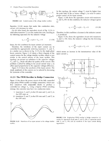
11.2.5 The PWM Rectifier in Bridge Connection i s L P i s L N
Figure 11.24a shows the power circuit of the fully controlled v L v L
+ +
single-phase PWM recti®er in bridge connection, which uses v C v C
s V s V
four transistors with antiparallel diodes to produce a 0 0
controlled dc voltage V . Using a bipolar PWM switching
o
strategy, this converter may have two conduction states: N P
b) c)
i) transistors T and T in the ON state and T and T in
4
3
2
1
the OFF state; or v ,i
s s
ii) transistors T and T in the ON state and T and T in v s i s
1
4
2
3
the OFF state.
v ,i
s s
v t
s
t
d)
i s
FIGURE 11.24 Single-phase PWM recti®er in bridge connection: (a)
circuit; (b) equivalent circuit with T 1 and T 4 ON; (c) equivalent circuit
FIGURE 11.23 Waveform of the input current in the voltage doubler with T 2 and T 3 ON; and (d) waveform of the input current during
recti®er. regeneration.