Page 189 - Rashid, Power Electronics Handbook
P. 189

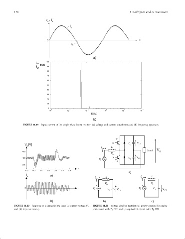
178                                                                           J. Rodrõ Âguez and A. Weinstein

                                    v ,i
                                      s  s
                                                     i
                                                     s


                                     0                                                             t
                                                     v
                                                      s


                                                                    a)
                              i      100
                              sn
                              i  100  90
                               s1
                                     80
                                     70
                                     60
                                     50
                                     40
                                     30
                                     20
                                     10
                                      0
                                        0           1            2           3           4           5
                                       10          10          10          10          10           10
                                                                   f [Hz]
                                                                    b)
                     FIGURE 11.19  Input current of the single-phase boost recti®er: (a) voltage and current waveforms; and (b) frequency spectrum.


                                                                                   T
                                                                                    1
                                                                                 X          C    V
                      V [V]                                                                  1     C1
                        o
                                                                         i      L
                                                                          s
                                                                                                        Load   V
                     415                                                                                        0
                                                                                v
                                                                                 L
                                                                           +     X
                     400                                                v                   C    V C2
                                                                         s         T         2
                                                                                    2
                     385
                                                          t
                       0.2  0.3  0.4  0.5  0.6  0.7  0.8
                                                                                            a)
                        i               a)
                        s                                                                           i      L
                                                                     i       L
                                                                      s                             s
                                                                            v                              v
                                                                             L                              L
                                                                      +                              +
                      0                                   t         v                              v        C
                                                                     s        C 1   V               s        2     V
                                                                                     C1                             C2
                                        b)                                 b)                              c)
               FIGURE 11.20  Response to a change in the load: (a) output-voltage V o ;  FIGURE 11.21  Voltage doubler recti®er: (a) power circuit; (b) equiva-
               and (b) input current i s .                          lent circuit with T 1 ON; and (c) equivalent circuit with T 2 ON.
   184   185   186   187   188   189   190   191   192   193   194