Page 174 - Rashid, Power Electronics Handbook
P. 174

10  Diode Recti®ers                                                                                 163

                                                                            and IðLSÞ falls to zero at t ¼ðD þ D ÞT.As
                                                                                                                 2
                                                                            D V ¼ V ðN =N ÞD,
                                                                                        S
                                                                                           P
                                                                                    IN
                                                                              2
                                                                                o
                                                                                                 V IN  N S
                                                                                            D ¼        D          ð10:105Þ
                                                                                             2
                                                                                                 V o  N P
                                                                            D is effectively the duty cycle of the output recti®er
                                                                              2
                                                                            D .
                                                                              R
                                                                          3. For ðD þ D ÞT < t < T
                                                                                      2
                                                                            The output recti®er D is off.
                                                                                              R
                                                                            The output capacitor C provides the output current
                                                                                                L
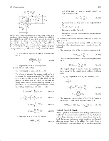
                 FIGURE 10.35  Practical forward converter with snubber circuits across  to the load R .
                                                                                       L
                 transformer and recti®ers: V IN ¼ 50 V; D M ¼ MUR460; D R ¼ MBR2540;
                                                                      The switching cycle restarts when the switch M is turned on
                 D F ¼ MBR2540; M 1 ¼ IRF640; R 1 ¼ 24 O; R 2 ¼ 10 O; R 3 ¼ 10 O;                            1
                 C 1 ¼ 3000 pF;  C 2 ¼ 10 nF;  C 3 ¼ 10 nF;  C L ¼ 3500 mF;  ESR  of  again at t ¼ T.
                 C L ¼ 0:05 O;  L 1 ¼ 8 mH;  L P ¼ 0:576 mH;  L M ¼ 0:576 mH;  From the waveforms shown in Fig. 10.39, the following
                 L S ¼ 0:036 mH; N P : N M : N S ¼ 4 : 4 : 1; effective winding resistance of  information (for discontinuous-mode operation) can be
                 L P ¼ 0:1 O; effective winding resistance of L M ¼ 0:4 O; and effective  obtained:
                 winding resistance of L S ¼ 0:01 O; and coupling coef®cient K ¼ 0:996.
                                                                          The maximum value of the current in the switch M is
                                                                                                                     1
                        The current in M , denoted as IDðM Þ, increases at the                      V IN
                                                     1
                                      1
                        rate of                                                          IDðM Þ   ¼  L  DT        ð10:106Þ
                                                                                             1 max
                                                                                                     P
                                                                          The maximum value of the current in the output recti®er
                                       dIDðM Þ  ¼  V IN       ð10:99Þ
                                             1
                                                                            R
                                          dt      L                       D is
                                                   P
                                                                                              N V  IN
                                                                                                P
                        The output recti®er D is reversely biased.                  IðDRÞ max  ¼  N  L  DT        ð10:107Þ
                                          R
                     2. For DT < t < ðD þ D ÞT                                                  S  P
                                          2
                                                                          The output voltage V can be found by equating the
                                                                                             o
                        The switching M is turned off at t ¼ DT.          input energy to the output energy within a switching
                                     1
                                                                          cycle
                        The collapse of magnetic ¯ux induces a back emf in L
                                                                   S
                        to turn on the output recti®er D . The initial ampli-
                                                   R                         V IN   ‰Charge taken from V in a switching cycle
                                                                                                    in
                        tude of the recti®er current IðDRÞ, which is also
                        denoted as IðLSÞ, can be found by equating the            V o 2
                                                                                ¼    T
                        energy stored in the primary-winding current IðLPÞ         R L
                        just before t ¼ DT to the energy stored in the second-                         2
                        ary-winding current IðLSÞ just after t ¼ DT:               V IN  1  DT  DT  V IN  ¼  V o  T  ð10:108Þ
                                                                                       2    L P      R L
                                 1       2   1       2
                                  L ðIðLPÞÞ ¼ L ðIðLSÞÞ      ð10:100Þ                       s 
                                   P
                                               S
                                 2           2                                               R T
                                                                                              L
                                                                                       V ¼       DV IN            ð10:109Þ
                                                                                        o
                                          2                                                   2L P
                             1    V IN       1       2
                               L P   DT    ¼ L ðIðLSÞÞ       ð10:101Þ
                                               S
                             2    L P        2                            The maximum reverse voltage of D ,Vð6; 9Þ (which is
                                                                                                        R
                                                                          the voltage at node 6 with respect to node 9), is
                                             s 
                                              L V  IN                                                  N
                                               P
                                      IðLSÞ¼        DT       ð10:102Þ         VðDRÞ    ¼ Vð6; 9Þ  ¼ V   S  þ V    ð10:110Þ
                                              L S  L P                              max        max   IN  N P  o
                                             N V IN                   10.6.2.2 Practical Circuit
                                              P
                                      IðLSÞ¼       DT        ð10:103Þ
                                             N S  L P                 When a practical transformer (with leakage inductance) is
                                                                      used in the ¯yback converter circuit shown in Fig. 10.38, there
                        The amplitude of IðLSÞ falls at the rate of   will be large ringings. In order to reduce these ringings to
                                                                      levels that are acceptable under actual conditions, snubber and
                                        dIðLSÞ  ÿV o                  clamping circuits have to be added. Fig. 10.40 shows a
                                              ¼              ð10:104Þ
                                          dt     L S                  practical ¯yback converter circuit where a resistor-capacitor
   169   170   171   172   173   174   175   176   177   178   179