
Page 322 - Satellite Communications, Fourth Edition
P. 322
302 Chapter Ten
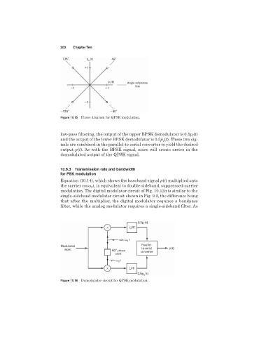
Figure 10.15 Phase diagram for QPSK modulation.
low-pass filtering, the output of the upper BPSK demodulator is 0.5p (t)
i
and the output of the lower BPSK demodulator is 0.5p (t). These two sig-
q
nals are combined in the parallel-to-serial converter to yield the desired
output p(t). As with the BPSK signal, noise will create errors in the
demodulated output of the QPSK signal.
10.6.3 Transmission rate and bandwidth
for PSK modulation
Equation (10.14), which shows the baseband signal p(t) multiplied onto
the carrier cos t, is equivalent to double-sideband, suppressed-carrier
0
modulation. The digital modulator circuit of Fig. 10.12a is similar to the
single-sideband modulator circuit shown in Fig. 9.2, the difference being
that after the multiplier, the digital modulator requires a bandpass
filter, while the analog modulator requires a single-sideband filter. As
Figure 10.16 Demodulator circuit for QPSK modulation.