
Page 319 - Satellite Communications, Fourth Edition
P. 319
Digital Signals 299
When p(t) 1, e(t) cos t, and when p(t) 1, e(t) cos t, which
0
0
is equivalent to cos( t 180°). Bandpass filtering of the modulated
0
wave may be used instead of baseband filtering to limit the radiated
spectrum. The bandpass filter also may incorporate the square root of
the raised-cosine rolloff, described in Sec. 10.5, required to reduce ISI
(see, for example, Pratt and Bostian, 1986).
At the receiver (Fig. 10.12b), the received modulated carrier will
undergo further bandpass filtering to complete the raised-cosine
response and to limit input noise. The filtered modulated wave,
er (t) pr (t) cos t , is passed into another multiplier circuit, where it is
0
t. The output from the
multiplied by a replica of the carrier wave cos 0
2
multiplier is therefore equal to pr (t) cos 0 t . This can be expanded as
pr (t) (0.5 0.5 cos 2 t) . The low-pass filter is used to remove the second
0
harmonic component of the carrier, leaving the low-frequency output,
which is 0.5p′(t), where p′(t) is the filtered version of the input binary
wave p(t). It will be seen that the modulator is basically the same as that
used to produce the DSBSC signal described in Sec. 9.3. In the present
instance, the bandpass filter following the modulator is used to select
the complete DSBSC signal rather than a single sideband.
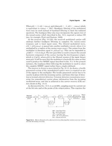
The receiver is shown in more detail in Fig. 10.13. As shown, a locally
generated version of the unmodulated carrier wave is required as one
of the inputs to the multiplier. The locally generated carrier has to be
exactly in phase with the incoming carrier, and hence this type of detec-
tion is termed coherent detection. Coherent detection necessitates recov-
ering the unmodulated carrier phase information from the incoming
modulated wave, and this is achieved in the carrier recovery (CR) sec-
tion shown in Fig. 10.13.
As discussed in Sec. 10.5, to avoid ISI, sampling must be carried out
at the bit rate and at the peaks of the output pulses. This requires the
Figure 10.13 Block schematic of a coherent detector showing the carrier recovery section
and the bit timing recovery.