
Page 329 - Satellite Communications, Fourth Edition
P. 329
Digital Signals 309
n
where Q 2 is the number of quantized steps, and n is the number of
bits per sample.
The BER can be improved through the use of error control coding. This
is the topic of Chap. 11.
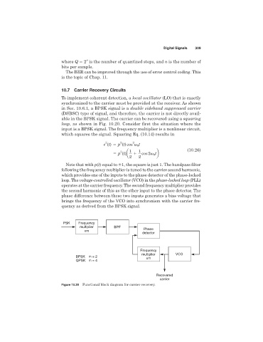
10.7 Carrier Recovery Circuits
To implement coherent detection, a local oscillator (LO) that is exactly
synchronized to the carrier must be provided at the receiver. As shown
in Sec. 10.6.1, a BPSK signal is a double sideband suppressed carrier
(DSBSC) type of signal, and therefore, the carrier is not directly avail-
able in the BPSK signal. The carrier can be recovered using a squaring
loop, as shown in Fig. 10.20. Consider first the situation where the
input is a BPSK signal. The frequency multiplier is a nonlinear circuit,
which squares the signal. Squaring Eq. (10.14) results in
2
2
2
e (t) p (t) cos t
0
2
p (t)a 1 1 cos 2 tb (10.26)
0
2 2
Note that with p(t) equal to 1, the square is just 1. The bandpass filter
following the frequency multiplier is tuned to the carrier second harmonic,
which provides one of the inputs to the phase detector of the phase-locked
loop. The voltage-controlled oscillator (VCO) in the phase-locked loop (PLL)
operates at the carrier frequency. The second frequency multiplier provides
the second harmonic of this as the other input to the phase detector. The
phase difference between these two inputs generates a bias voltage that
brings the frequency of the VCO into synchronism with the carrier fre-
quency as derived from the BPSK signal.
PSK Frequency
multiplier BPF
xm Phase
detector
Frequency
multiplier VCO
BPSK m = 2 xm
QPSK m = 4
Recovered
carrier
Figure 10.20 Functional block diagram for carrier recovery.