
Page 331 - Satellite Communications, Fourth Edition
P. 331
Digital Signals 311
Demodulated
signal Detector
A B Threshold output
Sampler decision
circuit
Zero-
crossing
LPF Squarer BPF detector
( ) 2
and clock
circuit
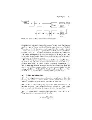
Figure 10.21 Functional block diagram for bit-timing recovery.
shown in block schematic form in Fig. 10.21 (Franks, 1980). The filters A
and B form part of the normal signal filtering (e.g., raised-cosine filtering).
The signal for the bit timing recovery is tapped from the junction between
A and B and passed along a separate branch which consists of a filter, a
squaring circuit, and a bandpass filter which is sharply tuned to the clock
frequency component present in the spectrum of the squared signal. This
is then used to synchronize the clocking circuit, the output of which clocks
the sampler in the detector branch.
The early-late gate circuit provides a method of recovering bit timing
which does not rely on a clocking component in the spectrum of the
received waveform. The circuit utilizes a feedback loop in which the
magnitude changes in the outputs from matched filters control the fre-
quency of a local clocking circuit (for an elementary description see, for
example, Roddy and Coolen, 1995). Detailed analyses of these and other
methods will be found in Franks (1980) and Gagliardi (1991).
10.9 Problems and Exercises
10.1. For a test pattern consisting of alternating binary 1s and 0s, determine
the frequency spectra in terms of the bit period T b for the following signal
formats: (a) unipolar; (b) polar NRZ; (c) polar RZ; (d) Manchester.
10.2. Plot the raised-cosine frequency response Eq. (10.9), for a bit rate of 1 b/s
and a roll of factor of 1, for a symbol rate equal to the bit rate. Use the inverse
Fourier transform to determine the shape of the pulse time waveform.
10.3. Plot the compressor transfer characteristics for 100 and A 100.
The -law compression characteristic is given by
ln(1 Zv i Z)
v sign(v i )
0
ln(1 )