
Page 411 - Satellite Communications, Fourth Edition
P. 411
The Space Link 391
energy, or E < hc/l. On this basis it turns out that silicon is useful for
G
wavelengths shorter that 1 m. Germanium is useful at 1.3 m and InSb
and InAs at 1.55 m.
The total current flowing in a photodiode consists of the actual cur-
rent generated by the photons, plus what is termed the dark current.
This is the current that flows even when no signal is present. Ideally it
should be zero, but in practice it is of the order of a few nanoamperes,
and it can contribute to the noise. Denoting the dark current by I the
d
total current is
I
I I ph d (12.68)
This current is accompanied by shot noise (a name that is a hangover
from vacuum tube days), the mean square spectral density of which is
2
2qI in A /Hz with I in amperes. This would be for a diode without any
internal amplification such as a PIN diode. An avalanche photo diode
(APD) multiplies the signal current by a factor M and at the same time
generates excess noise, represented by an excess noise factor, F, so that
the mean square spectral density is (2qI)MF. F increases with increase
in M (see Jones, 1988, p. 240). Typical values are of the order M 100,
F 12. For a PIN diode, M 1 and F 1.
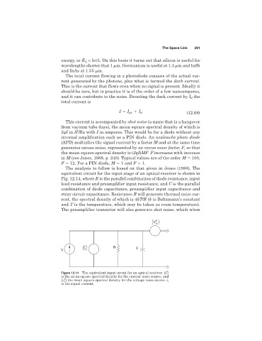
The analysis to follow is based on that given in Jones (1988). The
equivalent circuit for the input stage of an optical receiver is shown in
Fig. 12.14, where R is the parallel combination of diode resistance, input
load resistance and preamplifier input resistance, and C is the parallel
combination of diode capacitance, preamplifier input capacitance and
stray circuit capacitance. Resistance R will generate thermal noise cur-
rent, the spectral density of which is 4kT/R (k is Boltzmann’s constant
and T is the temperature, which may be taken as room temperature).
The preamplifier transistor will also generate shot noise, which when
V 2
a
i s i 2 t R C
2
Figure 12.14 The equivalent input circuit for an optical receiver. {i t }
is the mean square spectral density for the current noise source, and
2
{v a } the mean square spectral density for the voltage noise source. i s
is the signal current.