
Page 140 - Semiconductor For Micro- and Nanotechnology An Introduction For Engineers
P. 140
Periodic Potentials in Crystal
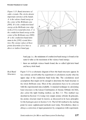
Figure 3.13. Band structures of
cubic crystals. The circles denote
important extremes of the bands.
A is the valence band energy at
the center of the Brillouin zone
B
[000]. is the conduction band C
energy at the Brillouin zone edge B
D
in the [111] crystal direction. is A
C
the conduction band energy at the
center of the Brillouin zone [000].
D is the conduction band mini-
mum in the [100] crystal direc-
tion. The energy values of these
points determine if we have a L [111] Γ [100] X K [110] Γ
direct or indirect band gap.
band gap, i.e., the minimum of conduction band energy is found at the
same k value as the maximum of the valence band energy;
• there are multiple valence bands found, the so called light-hole band
and heavy-hole band.
Real Band Figure 3.13 is a schematic diagram of how the band structures appear. In
Structures fact, nobody can tell either by experiment or calculation exactly what the
upper edge of the conduction band looks like. The calculations need
assumptions that might not be enough to determine the band structure in
the whole Brillouin zone. Most of the calculations have to be corrected
with the experimental data available. A standard technique in calculating
band structures is the Linear Combination of Atomic Orbitals (LCAO),
also called the tight binding method, see Box 3.1. This method was
sketched in Section 3.3.2 using very simple atomic orbitals. In principle,
the atomic structure must be known, as discussed in its basic principles
for the hydrogen atom in Section 3.2.6. The LCAO method is the starting
point for more sophisticated methods used today. Nevertheless, there is
always a correction of input parameters by comparison with experiment.
Semiconductors for Micro and Nanosystem Technology 137