Page 141 - Semiconductor For Micro- and Nanotechnology An Introduction For Engineers
P. 141

The Electronic System
                Box 3.1. The tight binding LCAO method [3.6]–[3.8].
                 Tight Binding. If we make the bold assumption   G =  V g  G =  V g
                                                         1   ss 1    2   sx 2 
                 that the wavefunctions of crystal atoms are only           
                                                       G =  V g     G =  V g
                                                                         sx 4 
                                                         3
                                                             sx 3
                                                                     4
                 slightly perturbed from their free state, and we              (B 3.1.4)
                                                       G =  V g     G =  V g 
                 severely limit the interaction between atoms to   5  xx 1  6  xy 2 
                 those of nearest neighbors only, and we only con-  G =  V g  G =  V g 
                                                         7
                                                                     8
                                                                         xy 4
                                                             xy 3
                 sider the most essential of the “free” atom’s orbit-  The Hamiltonian matrix now becomes
                 als, then a particularly straightforward calculation
                                                            E  G   0   0  0 G G G
                 of the crystalline band structure becomes possible   s  1    2  3  4
                 that correctly predicts the bands of the tightly-  G ∗  E s  – G – G – G 4  0  0  0
                                                            1
                                                                    2
                                                                        3
                 bound valence electrons.                   0 – G ∗ E  p  0  0 G G G 6
                                                                2
                                                                              5
                                                                                8
                 Hamiltonian. The crystal electron’s Hamiltonian   0 – G ∗  0  E p  0 G G G 7
                                                                                5
                                                                3
                                                                              8
                              2
                 is written as H =  p ⁄  2m +  k ∑  V r()  . We   H =  0 – G ∗  0  0  E  G G G
                                        k
                 assume that the basis states are the 3s   and 3 p  4      p  6  7  5
                                                           G ∗  0  G ∗ G ∗ G ∗ E  0  0
                 states. Since each of these four states ( ,   x  ,  p y  ,   2  5  8  6  p
                                          sp
                  p  z  ) can occur for each of the two Si sites in the   G ∗  0  G ∗ G ∗ G ∗ 0 E  p  0
                                                                       5
                                                                    8
                                                            3
                                                                          7
                 unit cell, the Hamiltonian will be an 8 ×  8   matrix.  G ∗  0  G ∗ G ∗ G ∗ 0  0 E  p
                                                            4
                                                                          5
                                                                    6
                                                                       7
                 Basis states. The crystal basis states are                     (B 3.1.5)
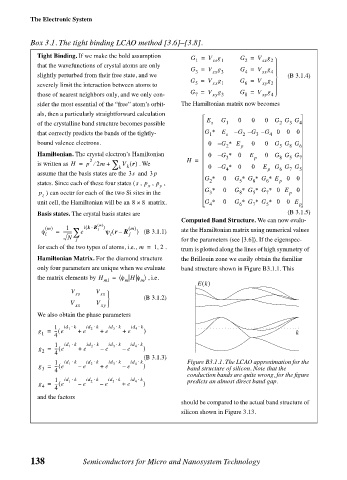
                                                     Computed Band Structure. We can now evalu-
                                ()
                                 m
                             (
                               ⋅
                        1
                    m
                                         m
                  φ ()  =  -------- ∑ e i kR j ) ψ r –  R () )  (B 3.1.1)  ate the Hamiltonian matrix using numerical values
                                    (
                   l               l    j
                                                     for the parameters (see [3.6]). If the eigenspec-
                         N j
                                               ,
                 for each of the two types of atoms, i.e., m =  12  .  trum is plotted along the lines of high symmetry of
                 Hamiltonian Matrix. For the diamond structure   the Brillouin zone we easily obtain the familiar
                 only four parameters are unique when we evaluate   band structure shown in Figure B3.1.1. This
                                          |
                 the matrix elements by H  =  φ 〈  |H φ 〉  , i.e.
                                  ml   m   m
                                                         Ek()
                          V     V
                           ss    sx 
                                           (B 3.1.2)
                          V     V
                           xx    xy 
                 We also obtain the phase parameters
                      1  id 1 k  id 2 k  id 3 k  id 4 k
                               ⋅
                                     ⋅
                          ⋅
                                          ⋅
                  g =  --- e (  +  e  +  e  +  e  )                               k
                  1   4
                                          ⋅
                                     ⋅
                          ⋅
                               ⋅
                      1  id 1 k  id 2 k  id 3 k  id 4 k
                  g =  --- e (  +  e  –  e  –  e  )
                  2   4
                                            (B 3.1.3)
                          ⋅
                               ⋅
                                          ⋅
                                     ⋅
                      1  id 1 k  id 2 k  id 3 k  id 4 k  Figure B3.1.1. The LCAO approximation for the
                  g =  --- e (  –  e  +  e  –  e  )
                  3   4                                band structure of silicon. Note that the
                                                       conduction bands are quite wrong, for the figure
                               ⋅
                                     ⋅
                                          ⋅
                          ⋅
                      1  id 1 k  id 2 k  id 3 k  id 4 k  predicts an almost direct band gap.
                  g =  --- e (  –  e  –  e  +  e  )
                  4
                      4
                 and the factors
                                                     should be compared to the actual band structure of
                                                     silicon shown in Figure 3.13.
                138          Semiconductors for Micro and Nanosystem Technology
   136   137   138   139   140   141   142   143   144   145   146