Page 244 - Semiconductor For Micro- and Nanotechnology An Introduction For Engineers
P. 244
Electron-Electron
                                              e
                                     ,,
                                   (
                                            ip---Ψ p z)∇ f E k()(
                                                                       (
                                                                         ,,
                               izδf kp z) +
                              –
                                                                    k
                                              —  (  ,  k 0     ) +  ipv δf kp z) =  0  (7.9)
                                                   (
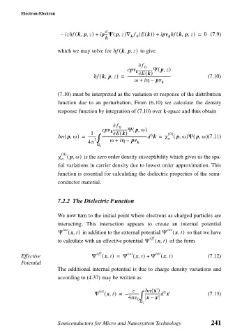
                             which we may solve for δf kp z)   to give
                                                    ,,
                                                         ∂f  0
                                                                  ,
                                                                (
                                                     epv       Ψ p z)
                                                         k ∂ E k()
                                             ,,
                                            (
                                          δf kp z) =  ----------------------------------------------  (7.10)
                                                        ω +  iη –  pv
                                                                  k
                             (7.10) must be interpreted as the variation or response of the distribution
                             function due to an perturbation. From (6.10) we calculate the density
                             response function by integration of (7.10) over k-space and thus obtain
                                                ∂f  0
                                                       (
                                                         ,
                                            epv       Ψ p ω)
                                        1       k ∂ E k()            0 ()
                                          3∫
                                                              3
                                 ,
                                                                        ,
                               (
                                                                               ,
                                                                             (
                             δn p ω) =  -------- ------------------------------------------------d k =  χ n  (  p ω)Ψ p ω) (7.11)
                                       4π      ω +  iη –  pv  k
                                           Ω k
                             χ  0 () (  p ω)   is the zero order density susceptibility which gives us the spa-
                                  ,
                              n
                             tial variations in carrier density due to lowest order approximation. This
                             function is essential for calculating the dielectric properties of the semi-
                             conductor material.
                             7.2.2 The Dielectric Function
                             We now turn to the initial point where electrons as charged particles are
                             interacting.  This interaction appears to create an internal potential
                              int
                                  ,
                                                                        ,
                             Ψ ( x t)   in addition to the external potential Ψ ext (  x t)   so that we have
                                                                 ,
                             to calculate with an effective potential Ψ eff  ( x t)   of the form
                                                                int
                                                                   ,
                                              ,
                                                         ,
                Effective                Ψ eff (  x t) =  Ψ ext ( x t) +  Ψ ( x t)  (7.12)
                Potential
                             The additional internal potential is due to charge density variations and
                             according to (4.37) may be written as
                                                       e
                                           int
                                          Ψ ( x t) =  – 4πε ∫  δn x'()  3         (7.13)
                                               ,
                                                      ----------- ----------------d x'
                                                               x'
                                                            x –
                                                         0
                                                          Ω r
                             Semiconductors for Micro and Nanosystem Technology    241

