Page 246 - Semiconductor For Micro- and Nanotechnology An Introduction For Engineers
P. 246
Electron-Electron
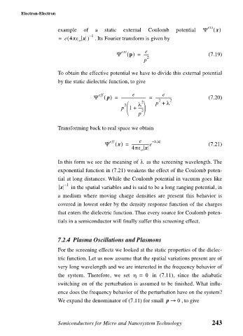
example of a static external Coulomb potential
(
= e 4πε x ) – 1 . Its Fourier transform is given by Ψ ext x ()
o
e
Ψ ext p () = ----- (7.19)
p 2
To obtain the effective potential we have to divide this external potential
by the static dielectric function, to give
e
e
Ψ eff () --------------------------- = ----------------- (7.20)
p =
2
2 p + λ 2
2 λ
p 1 + -----
2
p
Transforming back to real space we obtain
e
Ψ eff x () = ------------------e – λ x (7.21)
4πε x
o
λ
In this form we see the meaning of as the screening wavelength. The
exponential function in (7.21) weakens the effect of the Coulomb poten-
tial at long distances. While the Coulomb potential in vacuum goes like
– 1
x in the spatial variables and is said to be a long ranging potential, in
a medium where moving charge densities are present this behavior is
covered in lowest order by the density response function of the charges
that enters the dielectric function. Thus every source for Coulomb poten-
tials in a semiconductor will finally suffer this screening effect.
7.2.4 Plasma Oscillations and Plasmons
For the screening effects we looked at the static properties of the dielec-
tric function. Let us now assume that the spatial variations present are of
very long wavelength and we are interested in the frequency behavior of
the system. Therefore, we set η = 0 in (7.11), since the adiabatic
switching on of the perturbation is assumed to be finished. What influ-
ence does the frequency behavior of the perturbation have on the system?
We expand the denominator of (7.11) for small p → 0 , to give
Semiconductors for Micro and Nanosystem Technology 243

