Page 252 - Semiconductor For Micro- and Nanotechnology An Introduction For Engineers
P. 252
Electron-Phonon
                                                                       +
                                                             , while  b c
                             destroys a phonon with wavevector  q
                                                                           c
                                                 k
                                                                   –
                             electron with wavevector  , creates one with k q + – q k +  q k   destroys an
                                                                       and creates a phonon
                                          –
                             with wavevector  q  . This is why we call the first term phonon absorption
                             and the second one phonon emission. Thus the square of the matrix ele-
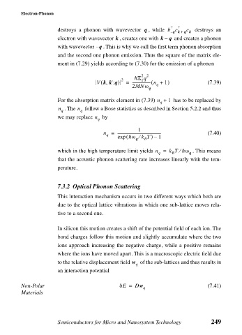
                             ment in (7.29) yields according to (7.30) for the emission of a phonon
                                                          2 2
                                                        —Ξ q
                                                   2
                                                          1
                                           V kk' q)  =  -------------------- n +(  1)  (7.39)
                                            (
                                              ,
                                                ;
                                                       2MNω     q
                                                             q
                             For the absorption matrix element in (7.39) n +  1   has to be replaced by
                                                                 q
                             n  . The n   follow a Bose statistics as described in Section 5.2.2 and thus
                              q      q
                             we may replace n   by
                                           q
                                                         1
                                             n =  -----------------------------------------------  (7.40)
                                              q
                                                  exp ( —ω ⁄  k T) –  1
                                                        q   B
                                                                        ⁄
                             which in the high temperature limit yields n =  k T —ω  . This means
                                                                 q   B      q
                             that the acoustic phonon scattering rate increases linearly with the tem-
                             perature.
                             7.3.2 Optical Phonon Scattering
                             This interaction mechanism occurs in two different ways which both are
                             due to the optical lattice vibrations in which one sub-lattice moves rela-
                             tive to a second one.
                             In silicon this motion creates a shift of the potential field of each ion. The
                             bond charges follow this motion and slightly accumulate where the two
                             ions approach increasing the negative charge, while a positive remains
                             where the ions have moved apart. This is a macroscopic electric field due
                             to the relative displacement field w   of the sub-lattices and thus results in
                                                         q
                             an interaction potential

                Non-Polar                          δE =  Dw                       (7.41)
                                                           q
                Materials


                             Semiconductors for Micro and Nanosystem Technology    249

