
Page 95 - Semiconductor Manufacturing Handbook
P. 95
Geng(SMH)_CH08.qxd 04/04/2005 19:41 Page 8.2
PHOTOMASK
8.2 SEMICONDUCTOR FUNDAMENTALS AND BASIC MATERIALS
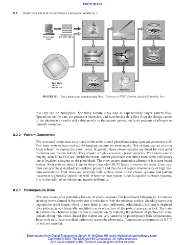
FIGURE 8.1 Basic photomask manufacturing flow. (Courtesy of ETEC Systems, Applied Materials, Inc.)
this step can be prodigious. Shrinking feature sizes lead to exponentially larger pattern files.
Operations on the data are processor intensive, and transferring data files from the design center
to the photomask vendor and subsequently to the pattern generation tools presents challenges to
network resources.
8.2.2 Pattern Generation
The converted design data are printed on the resist-coated photoblank using a pattern generation tool.
Two basic systems have evolved for imaging patterns on photomasks. One system uses an electron
beam (ebeam) to expose the photo resist. In general, these ebeam systems are noted for very good
resolution and pattern fidelity. They require a high vacuum to operate properly. Print times can be
lengthy, with 10 to 18 h not outside the norm. Pattern placement can suffer from beam deflections
due to localized charging on the photoblank. The other pattern generation alternative is a laser-based
system. Such systems utilize I-line or deep ultraviolet (DUV) lasers to expose the resist. Laser sys-
tems can operate at standard atmospheric pressure and thus do not require maintenance of high vac-
uum subsystems. Print times are generally half, or less, those of the ebeam systems, and pattern
placement is generally superior as well. Where the laser system is not as capable as ebeam systems,
it is in the realm of resolution and pattern uniformity.
8.2.3 Postexposure Bake
This step occurs after patterning for any of several reasons. For laser-based lithography, it removes
standing waves formed in the resist due to reflections from the substrate surface. Standing waves can
degrade the resist image, which in turn leads to poor uniformity. Additionally, this step is required
after patterning on chemically amplified resists regardless of the pattern generation tool. The bake
step drives the chemical amplification to completion by inducing the diffusion of photoactive com-
pounds through the resist. Resist line widths are very sensitive to postexposure bake temperatures.
Bake tools must have excellent uniformity across the photomask. Temperature uniformities of 0.5°C
or less are required.
Downloaded from Digital Engineering Library @ McGraw-Hill (www.digitalengineeringlibrary.com)
Copyright © 2004 The McGraw-Hill Companies. All rights reserved.
Any use is subject to the Terms of Use as given at the website.