
Page 99 - Semiconductor Manufacturing Handbook
P. 99
Geng(SMH)_CH08.qxd 04/04/2005 19:41 Page 8.6
PHOTOMASK
8.6 SEMICONDUCTOR FUNDAMENTALS AND BASIC MATERIALS
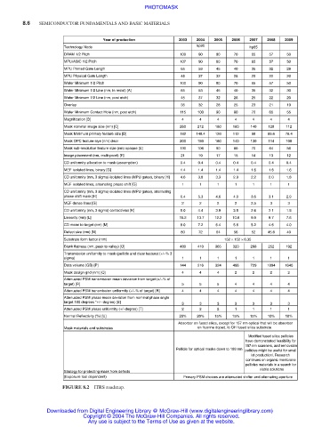
Year of production 2003 2004 2005 2006 2007 2008 2009
Technology Node hp90 hp65
DRAM 1/2 Pitch 100 90 80 70 65 57 50
MPU/ASIC 1/2 Pitch 107 90 80 70 65 57 50
MPU Printed Gate Length 65 53 45 40 35 32 28
MPU Physical Gate Length 45 37 32 28 25 22 20
Wafer Minimum 1/2 Pitch 100 90 80 70 65 57 50
Wafer Minimum 1/2 Line (nm, in resist) [A] 65 53 45 40 35 32 30
Wafer Minimum 1/2 Line (nm, post etch) 45 37 32 28 25 22 20
Overlay 35 32 28 25 23 21 19
Wafer Minimum Contact Hole (nm, post etch) 115 100 90 80 70 65 55
Magnification [B] 4 4 4 4 4 4 4
Mask nominal image size (nm) [C] 260 212 180 160 140 128 112
Mask Minimum primary feature size [D] 182 148.4 126 112 98 89.6 78.4
Mask OPC feature siye (nm) clear 200 180 160 140 130 114 100
Mask sub-resolution feature size (nm) opaque [E] 130 106 90 80 70 64 56
Image placement (nm, multi-point) [F] 21 19 17 15 14 13 12
CD uniformity allocation to mask (assumption) 0.4 0.4 0.4 0.4 0.4 0.4 0.4
MEF isolated lines, binary [G] 1.4 1.4 1.4 1.4 1.6 1.6 1.6
CD uniformity (nm, 3 sigma) isolated lines (MPU gates), binary [H] 4.6 3.8 3.3 2.9 2.2 2.0 1.8
MEF isolated lines, alternating phase shift [G] 1 1 1 1 1 1 1
CD uniformity (nm, 3 sigma) isolated lines (MPU gates), alternating
phase shift mask [H] 6.4 5.3 4.6 4.0 3.6 3.1 2.9
MEF dense lines [G] 2 2 2 2 2.5 3 3
CD uniformity (nm, 3 sigma) contact/vias [K] 5.0 4.4 3.9 3.5 2.6 2.1 1.8
Linearity (nm) [L] 15.2 13.7 12.2 10.6 9.9 8.7 7.6
CD mean to target (nm) [M] 8.0 7.2 6.4 5.6 5.2 4.6 4.0
Defect size (nm) [N] 80 72 64 56 52 45.6 40
Substrate form factor (mm) 152 × 152 × 6.35
Blank flatness (nm, peak to valley) [O] 480 410 365 320 298 252 192
Transmission uniformity to mask (pellicle and clear feature) (+/−% 3
sigma) 1 1 1 1 1 1 1
Data volume (GB) [P] 144 216 324 486 729 1094 1640
Mask design grid (nm) [Q] 4 4 4 2 2 2 2
Attenuated PSM transmission mean deviation from target (+/−% of
target) [R] 5 5 5 4 4 4 4
Attenuated PSM transmission uniformity (+/−% of target) [R] 4 4 4 4 4 4 4
Attenuated PSM phase mean deviation from nominal phase angle
target 180 degrees *+/− degree) [S] 3 3 3 3 3 3 3
Attenuated PSM phase uniformity (+/−degree) [T] 2 2 2 1 1 1 1
Normal Reflectivity (%) [U] 20% 20% 15% 15% 15% 10% 10%
Absorber on fused silica, except for 157 nm optical that will be absorber
Mask materials and substrates on fluorine doped, lo OH fused silica substrate.
Modified fused silica pellicles
have demonstrated feasibility for
157 nm scanners, and removable
Pellicle for optical masks down to 193 nm pellicles might be useful for small
lot productionl. Research
continues on organic membrane
pellicles materials in a search for
viable solutions
Strategy for protecting mask from defects
(Exposure tool dependent) Primary PSM choices are attenuated shifter and alternating aperture
FIGURE 8.2 ITRS roadmap.
Downloaded from Digital Engineering Library @ McGraw-Hill (www.digitalengineeringlibrary.com)
Copyright © 2004 The McGraw-Hill Companies. All rights reserved.
Any use is subject to the Terms of Use as given at the website.