Page 221 - Six Sigma for electronics design and manufacturing
P. 221
Six Sigma for Electronics Design and Manufacturing
                     188
                     termine  how  many  times  the  innerlayer  processing  rate  is  applied,
                     and the material cost of copper-clad dielectric and prepreg material
                     for adhesion of the layers. Since the drill cost rate is often expressed
                     per hole, this cost will depend on the stack height, which is in turn
                     based on the PCB thickness, hole diameter, and the required accuracy
                     of the location of the drilled hole. Too tight a hole tolerance, which af-
                     fects the solder mask operation, will result in a lower drilled stack,
                     and  therefore  higher  drilling  costs  but  less  misregistration  defects.
                     Most fabricators process full panels (such as the 18	 × 24	 size), so the
                     more images or PCBs that can be designed to fit on a single panel, the
                     smaller the PCB cost.
                       The cost of a fabricated PCB should provide a conversion process
                     from PCB design features to manufacturing cost. An important part
                     of this process is the designer’s understanding of the manufacturing
                     process, capabilities, and constraints. For example, the dry film solder
                     mask is the most expensive, yet offers the best quality in terms of sol-
                     dering defects in PCB assembly. The inverse is true of the screened
                     solder mask.
                       To calculate the effect of different design alternatives, a manufac-
                     turing engineer must provide information about each cost parameter
                     in the fabrication process that would influence the final cost. The cost
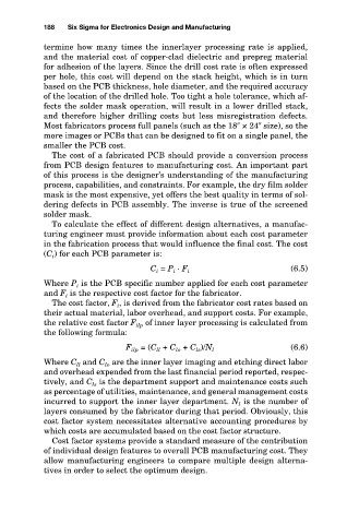
                     (C i ) for each PCB parameter is:
                                                                            (6.5)
                                             C i = P i · F i
                     Where P i is the PCB specific number applied for each cost parameter
                     and F i is the respective cost factor for the fabricator.
                       The cost factor, F i , is derived from the fabricator cost rates based on
                     their actual material, labor overhead, and support costs. For example,
                     the relative cost factor F ilp of inner layer processing is calculated from
                     the following formula:
                                                                            (6.6)
                                       F ilp = (C ll + C lo + C ls )/N l
                     Where C ll and C lo are the inner layer imaging and etching direct labor
                     and overhead expended from the last financial period reported, respec-
                     tively, and C ls is the department support and maintenance costs such
                     as percentage of utilities, maintenance, and general management costs
                     incurred to support the inner layer department. N l is the number of
                     layers consumed by the fabricator during that period. Obviously, this
                     cost factor system necessitates alternative accounting procedures by
                     which costs are accumulated based on the cost factor structure.
                       Cost factor systems provide a standard measure of the contribution
                     of individual design features to overall PCB manufacturing cost. They
                     allow manufacturing engineers to compare multiple design alterna-
                     tives in order to select the optimum design.

