
Page 216 - Six Sigma for electronics design and manufacturing
P. 216
183
Six Sigma Quality and Manufacturing Costs of Electronics Products
Mechanical Information
Electrical
Specifi-
PCB
PCB
PCB
Schematic
Design
Assembly
Fabrication
cations
Information
Analysis Layout Manufacturing Requirements
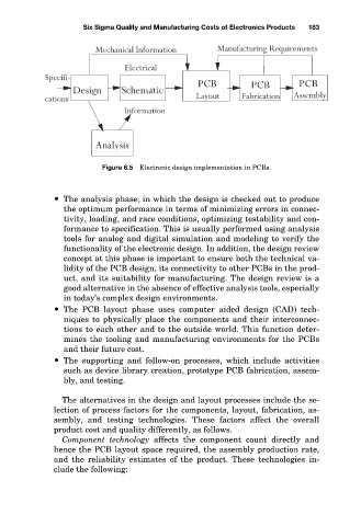
Figure 6.5 Electronic design implementation in PCBs.
The analysis phase, in which the design is checked out to produce
the optimum performance in terms of minimizing errors in connec-
tivity, loading, and race conditions, optimizing testability and con-
formance to specification. This is usually performed using analysis
tools for analog and digital simulation and modeling to verify the
functionality of the electronic design. In addition, the design review
concept at this phase is important to ensure both the technical va-
lidity of the PCB design, its connectivity to other PCBs in the prod-
uct, and its suitability for manufacturing. The design review is a
good alternative in the absence of effective analysis tools, especially
in today’s complex design environments.
The PCB layout phase uses computer aided design (CAD) tech-
niques to physically place the components and their interconnec-
tions to each other and to the outside world. This function deter-
mines the tooling and manufacturing environments for the PCBs
and their future cost.
The supporting and follow-on processes, which include activities
such as device library creation, prototype PCB fabrication, assem-
bly, and testing.
The alternatives in the design and layout processes include the se-
lection of process factors for the components, layout, fabrication, as-
sembly, and testing technologies. These factors affect the overall
product cost and quality differently, as follows.
Component technology affects the component count directly and
hence the PCB layout space required, the assembly production rate,
and the reliability estimates of the product. These technologies in-
clude the following: