
Page 452 - Solid Waste Analysis and Minimization a Systems Approach
P. 452
430 ELECTRONICS, SEMICONDUCTORS, AND OTHER ELECTRICAL EQUIPMENT
33.6 Case Study
The operations of high-tech companies are facing severe challenges from rapid chang-
ing of outside environment. The corporate vision should include the environmental
aspects and policies to ensure continuous growth of the operation. Besides, in order to
realize business globalization, it is required not only to develop high-quality products,
but also to implement environment management for the operation. Especially for most
of semiconductor companies, a strong environmental protection policy is inevitable as
a key factor for success of the manufacturing operation.
In 2003, a solid waste minimization study was conducted at a large semiconductor
manufacturing facility in California. The global company employs over 3500 individ-
uals and generated over $24 billion in 2007. At the time of the audit, the company was
pursuing new product and technology development as well as promotion and imple-
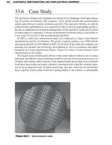
mentation of a waste minimization project. Figure 33.1 shows a semiconductor wafer
manufactured at the facility.
The largest waste minimization efforts in the semiconductor industry are in source
reduction. An effective source-reduction method is the use of acid spray processors for
cleaning and etching wafers instead of the standard batch processing in an acid bath.
Acid spray processing can reduce chemical consumption by using the cleaning chem-
ical in an on-demand mode. In batch processing, once the chemicals are mixed they
have a specific lifetime after which the cleaning ability of the solution is substantially
Figure 33.1 Semiconductor wafer.