
Page 121 - The Art and Science of Analog Circuit Design
P. 121
Analog Breadboarding
construction it is possible to consider likely causes of circuit malfunction
without wasting very much time.
In this chapter we shall consider some simple issues which are likely
to affect the success of analog breadboards, namely resistance (including
skin effect), capacitance, inductance (both self inductance and mutual
inductance), noise, and the effects of careless current routing. We shall
then discuss a breadboarding technique which allows us to minimize the
problems we have discussed.
Resistance
As an applications engineer I shall be relieved when room-temperature
superconductors are finally invented, as too many engineers suppose that
they are already available, and that copper is one of them. The assump-
tion that any two points connected by copper are at the same potential
completely overlooks the fact that copper is resistive and its resistance is
often large enough to affect analog and RF circuitry (although it is rarely
important in digital circuits).
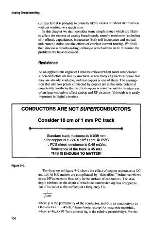
Consider 10 cm of 1 mm PC track
Standard track thickness is 0.038 mm
6
p for copper is 1.724 X 10" O cm @ 25°C
/. PCB sheet resistance is 0.45 mQ/sq
Resistance of the track is 45 mO
THIS IS ENOUGH TO MATTER!
Figure 9-2.
The diagram in Figure 9-2 shows the effect of copper resistance at DC
and LF. At HF, matters are complicated by "skin effect." Inductive effects
cause HF currents to flow only in the surface of conductors. The skin
depth (defined as the depth at which the current density has dropped to
1/e of its value at the surface) at a frequency f is
i
where }J, is the permittivity of the conductor, and o is its conductivity in
7
Ohm-meters. |i = 47ixlO' henry/meter except for magnetic materials,
7
where ^=4u\rcxlO- henry/meter (ji r is the relative permittivity). For the
104