
Page 205 - Troubleshooting Analog Circuits
P. 205
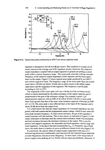
I92      C. Understanding and Reducing Noise on 3-Terminal Voltage Regulators


               Figure C.2.  Typical noise peaks produced by an LM3 I7 and various capacitive loads.


                         regulator is designed to roll off at 6 dB per octave. This condition is usually not of
                         much concern to the average user of IC regulator circuits. However, this inductive
                         output impedance coupled with an output capacitor to ground can produce a noise
                         peak within a narrow frequency range. This noise peak coincides with the resonant
                         frequency of the inductive output impedance of the regulator and the load capaci-
                         tance on the output. Figure C.2 shows typical noise peaks produced by an LM317
                         and various capacitive loads. The frequency range of the noise spike does not extend
                         much above 100  Wz nor below 10 lcHz due to ohmic losses in the added output
                         capacitance and the inductance of the regulator. The frequency is predictable
                         according to 1/(2  ra).
                           The magnitude of this noise spike will vary with the Q of the resonant circuit,
                         which is mainly dominated by the series resistance of the output capacitor and is
                         proportional to the gain of the reference voltage. For example, a good 1 p,F
                         polypropylene capacitor with an ESR of 20 mR at 30 kHz will have a noise peak
                         three times greater than that of the same value tantalum capacitor which has an ESR
                         of  1 or 2 R. The noise peak is also reflected back to the input of the regulator and is
                         about 20 dB down from the output level.
                           It is a little-known fact that the output impedance of 3-terminal regulators can vary
                         greatly with load current and the programmed output voltage, which in turn varies the
                         noise peak resonant frequency. As load current increases, the gm of the regulator’s
                         output transistor will also increase. This in turn causes, as indicated in Figure C.3, the
                         output inductance to decrease until the current-limit resistance, bond-wire resistance,
                         and lead resistance becomes the dominant resistance at the output. This is true for
                         positive and negative regulators, for adjustable and fixed regulators, and for large and
                         small regulators. In the past it has been assumed that ZOut vs. Frequency was a fixed
                         curve, but really there is a family of curves at different current levels (see Figure C.4).
                           In conclusion, the typical values of output bypass capacitance that users of 3-
                         terminal regulators have traditionally used may provide the expected noise reduction
                         at some frequencies, but not at every frequency. In most cases, a few microvolts of
                         power-supply noise peaking at 5 or 10 lcHz will not cause any problems. However, if