
Page 93 - Troubleshooting Analog Circuits
P. 93
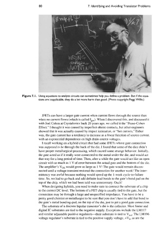
80                            7. Identifying and Avoiding Transistor Problems


               Figure 7. I.  Using equations to analyze circuits can sometimes help you define a problem. But if the equa-
                         tions are inapplicable, they do a lot more harm than good. (Photo copyright Peggi Willis.)


                           JFETs can have a larger gate current when current flows through the source than
                         when no current flows (which is called I&.  When I discovered this, and discussed it
                         with Joel Cohen at Crystalonics back 20 years ago, we called it the “Pease-Cohen
                         Effect.” I thought it was caused by imperfect ohmic contacts, but other engineers
                         showed that it was actually caused by impact ionization, or “hot carriers.” Either
                         way, the gate current has a tendency to increase as a linear function of source current,
                         with an exponential dependence on high drain-source voltages.
                           I recall working on a hybrid circuit that had some JFETs whose gate connection
                         was supposed to be through the back of the die. I found that some of the dice didn’t
                         have proper metallurgical processing, which caused some strange behavior. Initially,
                         the gate acted as if it really were connected to the metal under the die, and would act
                         that way for a long period of time. Then, after a while the gate would act like an open
                         circuit with as much as 1 V of error between the actual gate and the bottom of the die.
                         The amplifier’s  V,,  would grow as large as 1 V! The gate would remain discon-
                         nected until a voltage transient restored the connection for another week! The inter-
                         mittency was awful because nothing would speed up the 1-week cycle-to-failure
                         time. So, we had to go back and add definite lead bonds to the gate’s bond pad on the
                         top of the chip, which we had been told was unnecessary. Ouch!
                           When designing hybrids, you need to make sure to connect the substrate of a chip
                         to the correct DC level. The bottom of a FET chip is usually tied to the gate, but the
                         connection may be through a large and unspecified impedance. You have to be a
                         pretty good chemist or metallurgist to be sure that you don’t have to add that bond to
                         the gate’s metal bonding-pad, on the top of the die, just to get a good gate connection.
                           The substrate of a discrete bipolar transistor’s die is the collector. Most linear and
                         digital IC substrates are tied to the negative supply. Exceptions include the LM117
                         and similar adjustable positive regulators-their  substrate is tied to V,,,.  The LM196
                         voltage regulator’s substrate is tied to the positive supply voltage, +Vs, as are the