
Page 399 - Tunable Lasers Handbook
P. 399
8 Tunable External-Cavity Semiconductor Lasers 359
oxide- -contact Gain guided
cladding<< - active layer narrow stripe
oxide - 1 -contact
oxide - -contact Index guided
cladding4 -active layer ridge waveguide
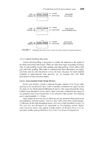
FIGURE 5 Schematic diode laser cross sections showing common waveguide structures
2.6.3 lateral Guiding Structures
Lateral optical guiding is necessary to confine the radiation ta the region of
the diode possessing optical gain. There are three basic types of guiding structures
(Fig. 5): gain guiding, strong index guiding, and ridge guiding. which utilizes both
gain and index guiding. The reader is cautioned that these illustrations are highly
schematic and are only intended to convey the basic structure. For more detailed
treatment of semiconductor laser structure. see, for example, Ref. [lo]. Brief
descriptions, of these structures follow.
2.6.3.1 Gain-Guided Oxide Stripe Devices
In this type of laser, current is injected through a narrow (5 to 10 pm wide)
opening in the top dielectric layer. Gain is laterally confined to the region around
the stripe by the limited lateral diffusion of carriers. The region beyond the stripe
exhibits large absorption losses, and so light is laterally confined to the region of
the pumping stripe even though there is no refractive index profile. The emitting
spot is approximately 1 x 10 pm.
Gain-guided devices are easy to fabricate and are therefore often used to test
semiconductor material quality. However, they suffer from three disadvantages:
(1 j Because of the high absorption losses, they have a high threshold current. (2)
The spot size and divergence are dependent on the pumping current. Higher
order transverse modes may appear at high current. (3) Because there is no lat-
eral index profile, gain-guided lasers have from 5 to 50 pm of astigmatism.