
Page 174 - A Comprehensive Guide to Solar Energy Systems
P. 174
Chapter 8 • Photovoltaics: The Basics 175
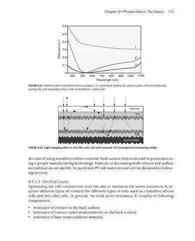
FIGURE 8.25 Reflectance of crystalline silicon surface [5,7]: plane bare surface (1), plane surface with antireflection
coating (2), and textured surface with antireflection coating (3).
FIGURE 8.26 Light trapping effect in thin film solar cell with textured TCO (transparent conducting oxide).
the case of using a multicrystalline material. such surface defects should be passivated us-
ing a proper manufacturing technology. Methods of decreasing both volume and surface
recombination are specific for particular PV cell materials and will be discussed in follow-
ing sections.
8.4.3.3 Electrical Losses
optimizing the cell construction with the aim to minimize the series resistance R s re-
quires different types of contacts for different types of cells such as crystalline silicon
cells and thin film cells. In general, the total series resistance R s consists of following
components:
• resistance of contact on the back surface;
• resistance of contact metal-semiconductor on the back surface;
• resistance of base semiconductor material;