
Page 171 - A Comprehensive Guide to Solar Energy Systems
P. 171
172 A CoMPrehensIVe GuIde To soLAr enerGy sysTeMs
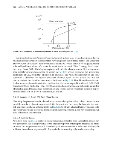
FIGURE 8.21 A comparison of absorption coefficients of silicon and GaAs (after Ref. [1,7]).
semiconductors with “indirect” energy band structure (e.g., crystalline silicon) have a
relatively low absorption coefficient for wavelengths in the infrared part of the spectrum.
Therefore, the thickness of the base material should be 150 µm or more for a high efficiency
solar cell and have a form of a wafer. In semiconductors with “direct” energy band struc-
ture (e.g., GaAs, CdTe, CuInse 2 , amorphous silicon), the absorption coefficient increases
very quickly with photon energy, as shown in Fig. 8.21, which compares the absorption
coefficient of GaAs with that of silicon. In this case, the whole useable part of the solar
spectrum is absorbed in a layer of thickness of about 3 µm. In such a case, the solar cell
can be realized in a thin film structure, as indicated in Fig. 8.22. Thin film cells can be real-
ized from amorphous silicon (or in combination with microcrystalline silicon), CdTe/Cds,
CuInse 2 (CIs), or Cu(In x Ga 1−x )se 2 (CIGs), deposited on a transparent substrate using thin
film techniques. details about construction and technology of cells from the most impor-
tant materials will be given in Chapters 9,10 and 18.
8.4.3 Losses in Real PV Cell Structures
Choosing the proper material, the cell structure can be optimized to collect the maximum
possible numbers of carriers generated. on the contrary, there may be losses in the solar
cell structure, as shown schematically in Fig. 8.23. To obtain a high efficiency in solar cells,
the construction and fabricated technology should be prepared in the way to minimize all
kind of losses in the structure.
8.4.3.1 Optical Losses
As follows from eq. (8.1), a part of incident radiation is reflected from the surface. excess car-
rier generation rate is proportional to the irradiative power entering the material. To maxi-
mize the carrier generation rate, it is necessary to minimize surface reflection. This may be
achieved in two basic ways—by thin film antireflection coating or by surface texturing.