
Page 206 - ARM Based Microcontroller Projects Using MBED
P. 206
192 8. INTERMEDIATE LEVEL PROJECTS
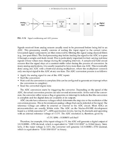
FIG. 8.54 Signal conditioning and ADC process.
Signals received from analog sensors usually need to be processed before being fed to an
ADC. This processing usually consists of scaling the input signal to the correct value.
Unwanted signal components are then removed by filtering the signal using classical filters
(e.g., low-pass filter). The final processing step before feeding the signal to the ADC is to pass
it through a sample-and-hold circuit. This is particularly important for fast varying real-time
signals whose values may change during the sampling intervals. A sample-and-hold circuit
ensures that the signal stays at a constant stable value during the process of conversion. In
many analog applications, it is usually required to have more than one ADC. This is normally
done using one ADC with a front-end analog multiplexer, where the multiplexer connects
only one input signal to the ADC at any one time. The ADC conversion process is as follows:
• Apply the analog signal to one of the ADC inputs
• Start the conversion
• Wait until the conversion is complete (this can be configured to generate an interrupt when
the conversion is complete)
• Read the converted digital data
The ADC conversion starts by triggering the converter. Depending on the speed of the
ADC, the actual conversion process can take several microseconds. At the end of the conver-
sion, the converter either raises a flag or generates an interrupt to indicate that the conversion
is complete and the digital data are available at its outputs.
ADC circuits have reference voltages which determine the step size or the resolution of the
conversion process. This is the minimum analog voltage that can be detected at the input. The
reference voltage can either be external or internal to the ADC circuit. Most ADCs on
microcontrollers are usually 10-bits wide. The ADC on the Nucleo-F411RE development
12
board is a 12-bit converter (2 ¼4096 quantization levels), having 16 channels and operating
with an internal reference voltage of +3.3V. The ADC resolution is, therefore, given by
+3:3V=4096 ¼ 0:00080V or 0:8mV
Therefore, for example, if the input voltage is 1V, the ADC will generate a digital output of
1.0/0.00080¼1250 decimal, which is equivalent to “0100 1110 0010” in 12-bit binary. Simi-
larly, if the input voltage is 3.0V, the converter will generate 3.0/0.00080¼3750 decimal,
which is equivalent to “1110 1010 0110” in binary.