
Page 53 - Advances in Renewable Energies and Power Technologies
P. 53
26 CHAPTER 1 Solar Cells and Arrays: Principles, Analysis, and Design
semiconductor device. This loss can be modeled by a shunt resistance (R sh ). Its effect
is much less visible in a solar cell compared with the series resistance. Now, the net
output current of the cell, considering both effects of R s and R sh , is given by
!
ðVþIRs Þ V þ IR s
I ¼ I ph I s e nV T 1 (1.43)
R sh
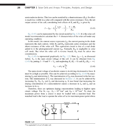
Eq. (1.43) can be represented by the circuit model in Fig. 1.21. It is the solar cell
model recommended to calculate the IeV characteristics of the solar cell under any
operating condition.
In this model, the current source represents I ph , the current passing in the diode
represents the dark current, while R s and R sh represents series resistance and the
shunt resistance of the solar cell. This equivalent circuit is that of a real diode
added to it the photogenerated current I ph .Normally R sh is negligible in solar
cell mode. But when the solar cell is reverse biased, R sh must be taken into
consideration.
Eq. (1.43) is represented graphically in Fig. 1.22. Here, I ph ¼ I sc as discussed
before. V oc is the open circuit voltage of the cell. It can be obtained from Eq.
(1.43) by putting I ¼ 0 and V ¼ V oc and neglecting R s (R s ¼ 0) and R sh (R sh ¼ N)
I ph
V oc ¼ nV T ln (1.44)
I s
The open circuit voltage of an electric source is its driving electromotive force. It
must be as high as possible. This can be achieved according to Eq. (1.44) by maxi-
mizing I ph and minimizing I s . The maximization of I ph was discussed in the last sec-
tion. The minimization of I s was discussed in Section 1.3. It can be achieved by
increasing N A , N D , L n , and L p and decreasing n j . It was found that increasing the
doping concentration of a semiconductor causes a decrease in L n and L p and an
increase in its n i .
Therefore, there are optimum doping concentrations leading to highest open
17
3
19
circuit voltage. For Si, e.g., N A ¼ 10 /cm and N D w 10 /cm 3. To draw the
maximum power from a source it must be loaded with a matched load. The
matched load is the load to operate the solar cell at its maximum power point where
FIGURE 1.21
The equivalent circuit of solar cell.