
Page 41 - An Introduction to Microelectromechanical Systems Engineering
P. 41
20 Materials for MEMS
Thin Metal Films
The choice of a thin metal film depends greatly on the nature of the final application.
Thin metal films are normally deposited either by sputtering, evaporation, or chemi-
cal vapor deposition; gold, nickel, and Permalloy™ (Ni Fe ), and a few other metals
x y
can also be electroplated. Table 2.3 lists some metals and conducting compounds
used as thin films, along with their resistivities (resistivity varies with deposition
conditions and is usually higher for thin films than for bulk material).
For basic electrical interconnections, aluminum (usually with a few percent
silicon and perhaps copper) is most common and is relatively easy to deposit by sput-
tering, but its operation is limited to noncorrosive environments and to temperatures
below 300ºC. For higher temperatures and harsher environments, gold, titanium,
and tungsten are substitutes. Aluminum tends to anneal over time and with tempera-
ture, causing changes in its intrinsic stresses. As a result, it is typically located away
from stress- or strain-sensing elements. Aluminum is a good light reflector in the visi-
ble, and gold excels in the infrared. Platinum and palladium are two very stable mate-
rials for electrochemistry, though their fabrication entails some added complexity.
Gold, platinum, and iridium are good choices for microelectrodes, used in electro-
chemistry and in sensing biopotentials. Silver is also useful in electrochemistry. Chro-
mium, titanium, and titanium-tungsten are frequently used as very thin (5–20 nm)
adhesion layers for metals that have poor adhesion to silicon, silicon dioxide, and sili-
con nitride. Metal bilayers consisting of an adhesion layer (e.g., chromium) and an
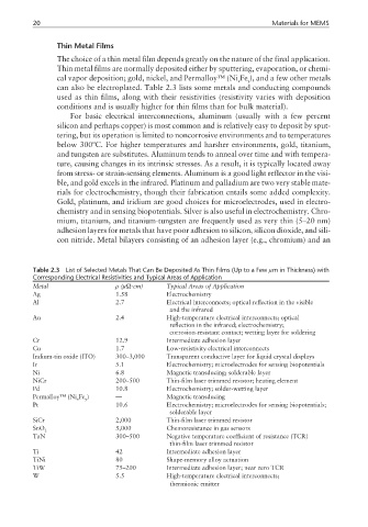
Table 2.3 List of Selected Metals That Can Be Deposited As Thin Films (Up to a Few µm in Thickness) with
Corresponding Electrical Resistivities and Typical Areas of Application
Metal ρ (µΩ·cm) Typical Areas of Application
Ag 1.58 Electrochemistry
Al 2.7 Electrical interconnects; optical reflection in the visible
and the infrared
Au 2.4 High-temperature electrical interconnects; optical
reflection in the infrared; electrochemistry;
corrosion-resistant contact; wetting layer for soldering
Cr 12.9 Intermediate adhesion layer
Cu 1.7 Low-resistivity electrical interconnects
Indium-tin oxide (ITO) 300–3,000 Transparent conductive layer for liquid crystal displays
Ir 5.1 Electrochemistry; microelectrodes for sensing biopotentials
Ni 6.8 Magnetic transducing; solderable layer
NiCr 200–500 Thin-film laser trimmed resistor; heating element
Pd 10.8 Electrochemistry; solder-wetting layer
Permalloy™ (Ni Fe ) — Magnetic transducing
x
y
Pt 10.6 Electrochemistry; microelectrodes for sensing biopotentials;
solderable layer
SiCr 2,000 Thin-film laser trimmed resistor
SnO 2 5,000 Chemoresistance in gas sensors
TaN 300–500 Negative temperature coefficient of resistance (TCR)
thin-film laser trimmed resistor
Ti 42 Intermediate adhesion layer
TiNi 80 Shape-memory alloy actuation
TiW 75–200 Intermediate adhesion layer; near zero TCR
W 5.5 High-temperature electrical interconnects;
thermionic emitter