
Page 38 - An Introduction to Microelectromechanical Systems Engineering
P. 38
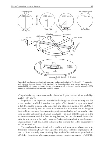
Silicon-Compatible Material System                                             17

                      Secondary flat                                           No secondary flat

                      (100) n-type    flat  (100) p-type      (111) n-type       (111) p-type
                                      Secondary  90°            45°


                                            Primary flat  Secondary flat         Primary flat
                                                               Primary flat
                      Primary flat
                                                       (a)
                                             (100) plane      (010) plane
                                     (110) plane
                           z, [001]                                       (001) plane
                      y, [010]
                                x, [100]
                                                                          [110] direction
                                  45 º


                                                                     (110)
                                                       (b)


                                        [001]        (111)
                                             [010]                 Surface
                                                                   is (001)
                                               (111)        (111)
                                                     (111)
                                             [100]
                                                        Flat is along [110] direction
                                                       (c)
                  Figure 2.2  (a) Illustration showing the primary and secondary flats of {100} and {111} wafers for
                  both n-type and p-type doping (SEMI standard); (b) illustration identifying various planes in a
                  wafer of {100} orientation (the wafer thickness is exaggerated); and (c) perspective view of a {100}
                  wafer and a KOH-etched pit bounded by {111} planes.


                  of impurity doping, but stresses tend to rise when dopant concentrations reach high
                  levels (~ 10 cm ).
                             20
                                 −3
                      Polysilicon is an important material in the integrated circuit industry and has
                  been extensively studied. A detailed description of its electrical properties is found
                  in [2]. Polysilicon is an equally important and attractive material for MEMS. It
                  has been successfully used to make micromechanical structures and to integrate
                  electrical interconnects, thermocouples, p-n junction diodes, and many other elec-
                  trical devices with micromechanical structures. The most notable example is the
                  acceleration sensor available from Analog Devices, Inc., of Norwood, Massachu-
                  setts, for automotive airbag safety systems. Surface micromachining based on poly-
                  silicon is today a well-established technology for forming thin (a few micrometers)
                  and planar devices.
                      The mechanical properties of polycrystalline and amorphous silicon vary with
                  deposition conditions, but, by and large, they are similar to that of single crystal sili-
                  con [3]. Both normally have relatively high levels of intrinsic stress (hundreds of
                  MPa) after deposition, which requires annealing at elevated temperatures (>900ºC).