
Page 35 - An Introduction to Microelectromechanical Systems Engineering
P. 35
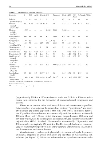
14                                                               Materials for MEMS

          Table 2.1  Properties of Selected Materials
          Property a    Si   SiO   Si N  Quartz SiC  Diamond  GaAs AlN  92% PolyimidePMMA
                                2   3  4
                                                                        Al O
                                                                          2  3
          Relative      11.7  3.9  4–8  3.75  9.7    5.7      13.1  8.5  9   —       —
           permittivity (ε )
                     r
          Dielectric    0.3  5–10  5–10  25–40 4     10       0.35  13  11.6  1.5–3  0.17
           strength
                   6
           (V/cm ×10 )
          Electron      1,500 —    —    —     1,000  2,200    8,800 —   —    —       —
           mobility
              2
           (cm /V·s)
          Hole mobility  400  —    —    —     40     1,600    400  —    —    —       —
              2
           (cm /V·s)
          Bandgap (eV)  1.12  8-9  —    —     2.3–3.2 5.5     1.42  —   —    —       —
          Young’s       160  73    323  107   450    1,035    75   340  275  2.5     3
           modulus (GPa)
          Yield/fracture  7  8.4   14   9     21     >1.2     3    16   15.4  0.23   0.06
           strength (GPa)
          Poisson’s ratio  0.22  0.17  0.25  0.16  0.14  0.10      0.31  0.31  0.34  —
                    3
          Density (g/cm )  2.4  2.2  3.1  2.65  3.2  3.5      5.3  3.26  3.62  1.42  1.3
          Coefficient of  2.6  0.55  2.8  0.55  4.2  1.0      5.9  4.0  6.57  20     70
           thermal
           expansion
             −6
           (10 /ºC)
          Thermal       157  1.4   19   1.4   500    990–2,000 0.46  160  36  0.12   0.2
           conductivity
           at 300K
           (W/m·K)
          Specific heat  0.7  1.0  0.7  0.787 0.8    0.6      0.35  0.71  0.8  1.09  1.5
           (J/g·K)
          Melting       1,415 1,700 1,800 1,610 1,800 b  3,652 b  1,237 2,470 1,800 380 c  90 c
           temperature (ºC)
          a
          Properties can vary with crystal direction, crystal structure, and grain size.
          b
          Sublimates before melting.
          c
          Glass transition temperature given for polymers.


                 (approximately $10 for a 100-mm-diameter wafer and $15 for a 150-mm wafer)
                 makes them attractive for the fabrication of micromechanical components and
                 systems.
                    Silicon as an element exists with three different microstructures: crystalline,
                 polycrystalline,or amorphous. Polycrystalline, or simply “polysilicon,” and amor-
                 phous silicon are usually deposited as thin films with typical thicknesses below 5
                 µm. Crystalline silicon substrates are commercially available as circular wafers with
                 100-mm (4-in) and 150-mm (6-in) diameters. Larger-diameter (200-mm and
                 300-mm) wafers, used by the integrated circuit industry, are currently economically
                 unjustified for MEMS. Standard 100-mm wafers are nominally 525 µm thick, and
                 150-mm wafers are typically 650 µm thick. Double-side-polished wafers commonly
                 used for micromachining on both sides of the wafer are approximately 100 µm thin-
                 ner than standard thickness substrates.
                    Visualization of crystallographic planes is key to understanding the dependence
                 of material properties on crystal orientation and the effects of plane-selective etch
                 solutions (see Figure 2.1). Silicon has a diamond-cubic crystal structure that can be