
Page 55 - An Introduction to Microelectromechanical Systems Engineering
P. 55
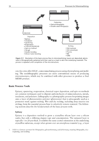
34                                                       Processes for Micromachining


                                                        Patterning
                                                   • Optical lithography
                         Photoresist               • Double-sided lithography
                         Thin film


                         Substrate
                             Deposition
                         • Epitaxy
                         • Oxidation
                         • Sputtering
                         • Evaporation
                         • CVD/LPCVD/PECVD                            Etching
                         • Spin-on method                           • Wet isotropic
                         • Sol-gel                                  • Wet anisotropic
                         • Anodic bonding                           • Plasma
                         • Silicon fusion bonding                   • RIE
                                                                    • DRIE
                 Figure 3.1  Illustration of the basic process flow in micromachining: Layers are deposited; photo-
                 resist is lithographically patterned and then used as a mask to etch the underlying materials. The
                 process is repeated until completion of the microstructure.


                 very few sites offer LIGA , a micromachining process using electroplating and mold-
                                       1
                 ing. The nonlithographic processes are more conventional means of producing
                 microstructures, which may be combined with other processes to produce a final
                 MEMS product.


          Basic Process Tools


                 Epitaxy, sputtering, evaporation, chemical-vapor deposition, and spin-on methods
                 are common techniques used to deposit uniform layers of semiconductors, metals,
                 insulators, and polymers. Lithography is a photographic process for printing images
                 onto a layer of photosensitive polymer (photoresist) that is subsequently used as a
                 protective mask against etching. Wet and dry etching, including deep reactive ion
                 etching, form the essential process base to selectively remove material. The follow-
                 ing sections describe the fundamentals of the basic process tools.

                 Epitaxy
                 Epitaxy is a deposition method to grow a crystalline silicon layer over a silicon
                 wafer, but with a differing dopant type and concentration. The epitaxial layer is
                 typically 1 to 20 µm thick. It exhibits the same crystal orientation as the underlying
                 crystalline substrate, except when grown over an amorphous material (e.g., a layer


          1.  LIGA is a German acronym for lithographie, galvanoformung, und abformung, meaning lithography, elec-
              troplating, and molding.