
Page 117 - Analog Circuit Design Art, Science, and Personalities
P. 117
Analog Design Discipline
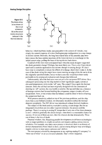
Figure 12-2.
The diode string:
(a) as shown on
the circuit
schematic;
(b) as the actual
device structures
behaved in the
thermal detector.
behavior, which had been totally unexplainable in the context of 3 diodes, was
simply the natural response of a slow Darlington pnp configuration to a step change
in emitter current. Basically, the long base transit time of the parasitic pnp struc-
tures causes the base-emitter junctions of the lower devices to overcharge on the
initial current edge. pulling the base of the top device back down.
Could all of this have been anticipated back when the mask designer suggested
the diode geometry change? Perhaps, but more likely not. This is why I have devel-
oped such a cautious approach to last minute changes in analog design. If I don’t
have time to completely evaluate the effects of a change. then I don’t make it. In the
case of the diode string this might have meant moving an edge of the die out to fit in
the originally specified diodes, but as we have seen this would have been vastly
preferable to the protracted evaluation and changes that followed.
Unfortunately, all of the bad news was not yet in for our power FET driver. On a
subsequent processing run the chip started to draw significant supply current at
elevated temperatures while in the ‘off‘ state. The culprit? Once again the thermal
detector. Since the cell had not been originally designed with the constraint of
drawing no ‘off’ current, this was hardly a surprise. But up until that run, a balance
of leakage currents had favored holding the comparator output circuitry off over
temperature. Now, it was evident that the balance could be tilted in favor of having
the output turn back on.
With process sensitivity added on top of the previous problems, and the chip
more than a year behind schedule, we reluctantly decided to defeat the thermal
detector completely. The FET driver was introduced without thermal shutdown.
The subject of this book and my example is analog circuit design. But for an
integrated circuit there are two other required elements: the process and the
package. There is a saying in analog IC design that if only one of the three elements
is new-which is generally the circuit design-then there is a reasonable chance for
success. If two out of three are new, then the chances decline dramatically. Three
out of three is the kiss of death.
Practical wisdom. this. Requiring parallel devclopments in different technologies
with no major problems is simply unrealistic and requires adding serious time to
schedules. For example, any time a new process is involved, there is no history of
device characteristics from which to draw, and an analog designer may unwittingly
require a device to meet specs a process can’t deliver.
The next project selected by management at my aspiring analog IC company? A
“three out of three” on an ucceleruted schedule. That’s when I departed.
98