
Page 53 - Analog Circuit Design Art, Science, and Personalities
P. 53
Reflections of a Dinosaur
Vcc (+I5 Volts)
Ri3
Switches
“SC
-
IOUt+
(-10 v01ts1-
10K
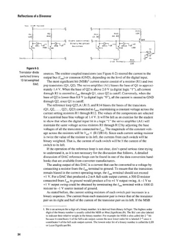
Figure 6-3.
Transistor-diode sources. The emitter coupled transistors (see Figure 6-2) steered the current to the
switched binary output bus (lout) or common (GND), depending on the level of the digital input.
weighted The most significant bit (MSB)’ current source consist of a resistor (Rl) and two
pnp transistors (41, 42). The servo amplifier (Al) biases the base of Q1 to approxi-
mately 1.4 V. When the base of 42 is above 2.0 V (a digital logic “I”), all current
through R 1 is steered to IOU, through Q 1, since 42 is cutoff. Conversely, when the
base of 42 is lower than 0.8 V (a digital logic “O“), all the current is steered to GND
through 42, since Q1 is cutoff.
The reference loop Q25,A 1 ,R 13, and R 14 biases the bases of the transistors
(Ql, 42,. . . ,42 I, Q23) connected to lout, maintaining a constant voltage across the
current setting resistors R 1 through R12. The values of the components are selected
for a nominal base bias voltage of I .4 V. It will be left as an exercise for the student
to show that when the digital input bit is a logic ‘‘I” the servo amplifier (AI) will
maintain the same voltage across resistors R1 through R12 by adjusting the base
voltages of all the transistors connected to lout. The magnitude of the constant volt-
age across the resistors will be VrCf X (R13/R14). Since each current setting resistor
is twice the value of the resistor to its left, the currents from each switch will be
binary weighted. That is, the current of each switch will be !4 the current of the
switch to its left.
If the operation of the reference loop is not clear, don’t spend serious time trying
to understand it, as it is not necessary for the discussion that follows. A detailed
discussion of DAC reference loops can be found in one of the data conversion hand-
books that are available from converter manufacturers.
The analog output of this DAC is a current that can be converted to a voltage by
connecting a resistor from the lout terminal to ground. To ensure that the transistors
remain biased in the correct operating range, the terminal should not exceed
+I V. For a DAC that produced a 2 mA full scale output current, a 500 SZ resistor
connected from I,,, to ground would produce a 0 to +I V output swing. A -1 V to
+I V output swing could be obtained by terminating the lo,,, terminal with a 1000 Cl
resistor to -I V source instead of ground.
As stated before, the current setting resistors of each switch pair increases in a
binary sequence. The current from each transistor pair is twice that of the transistor
pair on its right and half of the current of the transistor pair on its left. If the MSB
I. Bit is an acronym for a digii of a binary number. It is derived from Binary InTeger. The highest order
digit of the binary number is usually called the MSB or Most Significant Bit. The Bit‘s arc also labeled
to indicate their relative weight in the binary number. For example the MSB is also called the 2-I bit
because it contributes !4 of the full scale output current the next lower order bit is labeled 2-* since it
contributes !4 of the full scale output current. The lowesi order bit of a binary number is called the LSB
or Least Significant Bit.
34