
Page 58 - Analog Circuit Design Art, Science, and Personalities
P. 58
Samuel Wilensky
This design works as long the Zout is maintained at 2 V. The current from each
bit would flow to either the right- or left-hand diode, depending on the state of the
digital input. To maintain the proper digital switching level and to keep the current
through each bit constant, it is necessary to hold the Zout node at 2 V. This is
accomplished by using a transistor (Ql) as a constant voltage node to sum the
currents from each bit. The reference loop of Figure 6-2 is replaced by four diodes
(CR18,CR19,CR20,CR21), a zener reference (CR17), and a resistor (R9) (see
Figure 6-8). The reference circuit depends on the forward voltage across a diode
(CR19) tracking the V, of the transistor (Ql). This circuit compensates for V,
changes of the transistor with temperature, but it does not compensate for changes
in transistor beta. The reference circuit does not adjust as well as the servo loop,
but it is good enough. The reference circuit maintains a constant voltage across the
resistors (Rl,R2, . . ., R8), and the transistor sums the bit currents to the rout node.
Since the emitter-to-base voltage of the transistor varies with emitter current, the
linearity of the circuit was limited to slightly better than 8 bits (0.2%).
A schematic of the design of what became Hybrid Systems’ DAC 371-8 is shown
in Figure 6-8. The mechanical construction of the DAC 371-8 was also distinctive.
The diodes and resistors were mounted on end, resulting in a DAC footprint only
slightly larger than a 16 pin dual in-line integrated circuit package. The pins for the
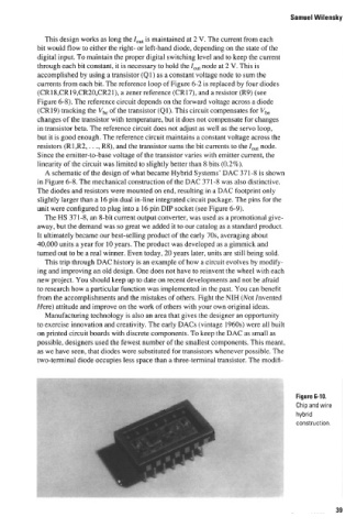
unit were configured to plug into a 16 pin DIP socket (see Figure 6-9).
The HS 371-8, an %bit current output converter, was used as a promotional give-
away, but the demand was so great we added it to our catalog as a standard product.
It ultimately became our best-selling product of the early 70s, averaging about
40,000 units a year for 10 years. The product was developed as a gimmick and
turned out to be a real winner. Even today, 20 years later, units are still being sold.
This trip through DAC history is an example of how a circuit evolves by modify-
ing and improving an old design. One does not have to reinvent the wheel with each
new project. You should keep up to date on recent developments and not be afraid
to research how a particular function was implemented in the past. You can benefit
from the accomplishments and the mistakes of others. Fight the NIH (Not Invented
Here) attitude and improve on the work of others with your own original ideas.
Manufacturing technology is also an area that gives the designer an opportunity
to exercise innovation and creativity. The early DACs (vintage 1960s) were all built
on printed circuit boards with discrete components. To keep the DAC as small as
possible, designers used the fewest number of the smallest components. This meant,
as we have seen, that diodes were substituted for transistors whenever possible. The
two-terminal diode occupies less space than a three-terminal transistor. The modifi-
Figure 6-10.
Chip and wire
hybrid
construction.
39