
Page 54 - Analog Circuit Design Art, Science, and Personalities
P. 54
Samuel Wilensky
Eight
1 i y
E~ua
k'elgnted
Swi tCheB
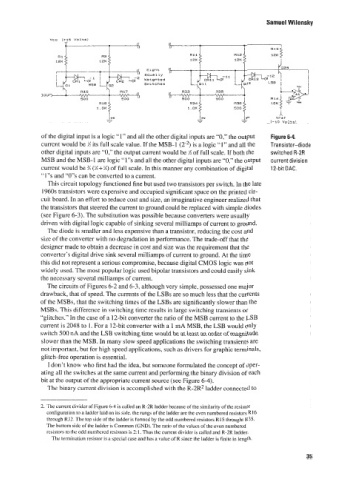
ofrhe digital input is a logic "1" and all the other digital inputs are "0,'' the output Figure 6-4.
currcnt would be X its full scale value. If the MSB-I (2-2) is a logic "1 " and all the Transistor-diode
other digital inputs are 'Y),'' the output current would be A of full scale. If both the switched R-2R
MSB and the MSB-1 are logic "1"s and all the other digital inputs are "0," the output current division
current would be .% (X+%) of full scale. In this manner any combination of digital 12-bit DAC.
'' 1 "s and "0"s can be convcrted to a current.
This circuit lopology functioned fine but used two transistors per switch. In the late
1960s transistors were expensive and occupied significant space on the printed cir-
cuit board. In an effort to reduce cost and size, an imaginative engineer realized thar
the transistors that steered the current to ground could be replaced with simple diodes
(see Figure 6-3). The substitution was possible because converters were usually
driven with digital logic capable of sinking several milliamps of current to ground.
The diode is smaller and less expensive than a transistor, reducing the cost and
six of the converter with no degradation in performance. 'The trade-off that the
designer made to obtain a dccrease in cost and size was the requirement that the
convertcr's digital drive sink several milliamps of current to ground. At the time
this did riot represent a serious compromise, because digital CMOS logic was not
widely used. The most popular logic used bipolar transistors and could easily sink
the necessary several milliamps of current.
The circuits of Figures 6-2 and 6-3, although very simple, possessed one major
drawback, that of speed. The currents of the LSRs are so much less that the currents
of the MSBs: that the switching times of the LSBs are significantly slower than the
MSBs. This difference in switching time results in large switching transients or
"glitches." In the case of a 12-bit converter the ratio of the MSB current to the LSB
current is 2048 to 1. For a 12-bit converter with a 1 mA MSB, the LSB would only
switch 500 nA and the LSB switching time would be at least an order of magnitude
slower than the MSB. In many slow speed applications the switching transients are
not important, but for high speed applications, such as drivers for graphic terminals,
glitch-free operation is essential.
I don't know who first had the idea, but someone formulated the concept of oper-
ating all the switches at the same current and performing the binary division of each
bit at ;:he output of the appropriate current source (see Figure 6-4).
The binary currcnt division is accomplished with the R-2R2 ladder connected to
2. The current divitlcr of Figure 6-4 is called an K-2K ladder becausc of the similarity of the resistor
conl'iguration to a ladder laid on its side. the rung3 of thc ladder are the even numbered resistors R I6
through K.2. The top bide of the ladder is fonnctl by the odd numbered resistors 1115 throught R35.
The hortom sidc of the ladder is Coininon (GND). The ratio of the valucs of the even numbered
rcsistors to the odd numhercd resistors is 2: I. Thus thc cument divider is called and R-2K ladder.
The lermination resistor is 21 spccial case and has a value of K since the ladder is finite in length.
35