Page 265 - Analog and Digital Filter Design
P. 265

262 Analog and Digital Filter Design


                       equalizer for this filter has a normalized  capacitor value of  2.0  that must  be
                       divided by  o.R, or 314,159. The capacitor required is 6.366pF. The equalizer’s
                       normalized inductor value is also 2.0. This must be multiplied by R and divided
                       by  o, which is a multiplying factor of  7.95775 x   The inductor required is
                       15.916mH: each half winding requires a self-inductance of  3.979  mH.
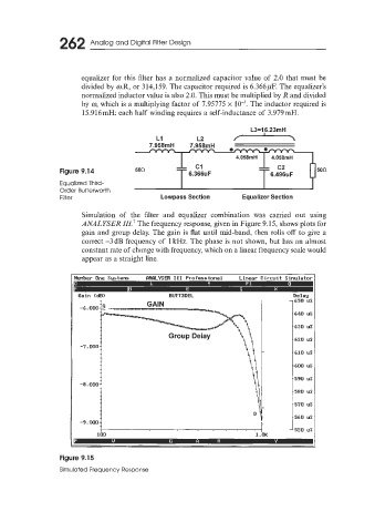
                                                                 *
                                                                      L3=16.23mH
                                            L1         L2


                 Figure 9.14                                                            500
                                                     6.366uF               6.496uF
                 Equalized Third-
                 Order Butterworth
                 Filter                      Lowpass Section       Equalizer Section

                       Simulation  of  the  filter  and  equalizer  combination  was  carried  out  using
                       ANALYSER III.’ The frequency response, given in Figure 9.15, shows plots for
                       gain and group delay. The gain is fiat until mid-band, then rolls off  to give a
                       correct -3dB  frequency of  1  kHz. The phase is not shown, but has an almost
                       constant rate of change with frequency, which on a linear frequency scale would
                       appear as a straight line.

                     m
                                                                   Linear  Circuit  Sinulatar
                                         ClNClLYSER  111  Professional
                     tunber  One  Srstens
                                                                                I
                      Gain  (dE)               BUTTBDEL                          Delay
                                                                                  650 US
                                                                                  640 US
                                                                                  630 US

                                                                                  620 US
                                                                                  610 US
                                                                                  600 US
                                                                                  590 US
                                                                                  580  us

                                                                                  570  US
                                                                                  560 US
                                                                                  550  US
                           100                                         1


                 Figure 9.15
                 Simulated Frequency Response
   260   261   262   263   264   265   266   267   268   269   270