
Page 151 - Antennas for Base Stations in Wireless Communications
P. 151
124 Chapter Three
a double-layer PCB, which has a thickness of 1.5 mm and a relative
permittivity of 2.65. A microstrip feeding line is printed on the upper
side of the same PCB. A coaxial cable with an outer diameter of 3.6mm
is also introduced to this antenna. Its outer conductor is used to connect
the lower patch and the ground plane together. On the other hand, its
inner conductor is bent to an L-shaped probe (upper probe) to couple
the energy to the upper patch for the upper-band operation. For the
lower-band operation, the lower patch is excited by another L-shaped
probe (lower probe) under it. The energy is delivered from one L-probe
to the other one through the microstrip feeding line. In Figure 3.21,
two cascaded low-pass filters, called compact microstrip resonant cell
11
(CMRC) , are integrated into the feeding line. Actually, they can effec-
tively suppress the excitation of higher-order modes of the lower-band
patch, which can affect the performance of the upper-band patch. The
antenna dimensions are detailed in the figure.
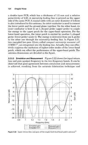
3.2.5.2 Simulation and Measurement Figure 3.22 shows the input return
loss and gain against frequency in the two frequency bands. It can be
observed that good agreement between simulation and measurement
is achieved, resulting from the accurate fabrication technique and
0 11
−2 10
−4 9
−6 8
Return Loss (dB) −10 7 Gain (dBi)
−8
6
−12
5
−14 4
−16 3
−18 2
−20 1
0.8 1 1.2 1.4 1.6 1.8 2 2.2
Frequency (GHz)
Simulated gain Measured gain
Simulated S11 Measured S11
Figure 3.22 Input return loss and gain of the single-feed dual-band patch antenna 10